Intro of PLL
Phase Detector
A phase detector is a circuit whose average output, $V_\tx{out}$ , is linearly proportional to the phase difference, $\Delta \phi$, between its two inputs (Fig. 16.1) The splope of the line is called the “gain” of the PD, $K_{PD}$

An example of a phase detecor is XOR gate(Fig. 16.2). However, the $\overline{V_\tx{out}} - \Delta \phi$ of XOR PD is not linear. (Fig. 16.3) (注意此处说的是平均输出电压)


补充,上面这个鉴相器的捕获范围(可正常工作的范围)是 $(0,\pi)$
Basic PLL Topology
锁相环的目标是使得输出的频率与输入的参考频率相同。你可能会有疑惑:为什么不直接用参考频率呢?emm……锁相环的用途没这么简单,它有三个主要用途:
- 频率综合:产生 K 倍于参考频率的信号
- 减小时钟偏移:数字系统中常用
- 时钟恢复:在一些信号传输系统中会用到
既然是让频率一致,那为什么不叫“锁频环”而叫锁相环呢?这就要从 PLL 的原理来解释。
假设 VCO 的相位 $\phi_\tx{out}$与标准时钟的相位 $\phi_\tx{in}$ 相差 $\Delta \phi$,我们知道相位是频率的积分 $\phi = \int \omega_\tx{out} \dif t = \int (\omega_0 + K_\tx{VCO}V_\tx{cont}) \dif t$,假设输出与输入频率相差 $\phi_\tx{out} - \phi_\tx{in} = \Delta \phi$,那么对相位微分就得到频率:
\[\omega_\tx{out} = \omega_\tx{in}+ \frac{\dif \Delta \phi}{\dif t}\\\]若我们能保持相位差恒定不变,即 $\dfrac{\dif \Delta \phi}{\dif t}=0$,那么 $\omega_\tx{out} = \omega_\tx{in}$。简单来说,就是通过相位锁定来实现频率锁定。
这么一来,我们可以画出一个简单的锁相环(Fig. 16.5a)为了滤除高频分量(避免抖动),我们在 PD 后面加一个低通滤波器(Fig. 18.5b)
%20Feedback%20loop%20comparing%20input%20and%20output%20phases;%20(b)%20simple%20PLL.jpg "Figure 16.5 (a) Feedback loop comparing input and output phases; (b) simple PLL")
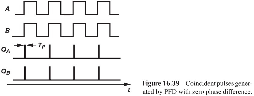
当锁相环锁定时($V_\tx{in}$ 和 $V_\tx{out}$ 频率相同,但有相位差),其波形如 Fig. 16.7a 所示(the PD produces pulses only on the rising transitions)。
%20Waveforms%20in%20a%20PLL%20in%20locked%20condition;%20(b)%20calculation%20of%20phase%20error.jpg "Figure 16.7 (a) Waveforms in a PLL in locked condition; (b) calculation of phase error")
Fig. 16.7b 为 VCO 和 PD 的输出特性,用公式表示为:
\[\begin{aligned} \omega_\tx{out} &= \omega_0 + K_{VCO}V_\tx{cont}\\ \overline{V_{PD}} &= K_{PD} \Delta \phi \end{aligned}\]若此时的振荡频率为 $\omega_1$,那么,我们求出 $V_1$ 和 $\phi_0$ 的值:
\[V_\tx{cont,dc} = V_1 = \frac{\omega_1-\omega_0}{K_{VCO}}\\ \begin{aligned} \phi_0 &= \frac{V_1}{K_{PD}}\\ &= \frac{\omega_1-\omega_0}{K_{PD}K_{VCO}} \end{aligned}\]从上面计算中,我们可以得出两个结论:
- 对于任意一个输入频率 $\omega_1$,都有唯一一个 $\phi_0$ 与之对应
- 要想减少 $\phi_0$,就要增大 $K_{PD}K_{VCO}$
若 VCO 和 PD 的特性如下图所示,问能否锁定?

当输入频率小于 $\omega_X$ 时,可以锁定,但当输入频率达到 $\omega_X$ 时,若要锁定,则必须有 $V_\tx{cont}=V_0$,但此时 $\dfrac{\dif \overline{V_\tx{out}}}{\dif \Delta \phi}=0$,说明此时 PD 的输出无法响应相位的变化,就会导致无法锁定。
尝试用数学语言描述如下:
$$
\omega_\tx{out} = \omega_0 + K_{VCO} f(\Delta \phi)\\
\Downarrow\\
\begin{aligned}
\frac{\dif \omega_\tx{out}}{\dif t} &= \frac{\dif \omega_0}{\dif t} + K_{VCO} \frac{\dif f(\Delta \phi)}{\dif t}\\
&=K_{VCO}\cdot \frac{\dif f(\Delta \phi)}{\dif \Delta \phi}\Bigg\vert_{v = V_0} \cdot \frac{\dif \Delta \phi}{ \dif t}\\
&=0
\end{aligned}\\
$$
The PD gain drops to zero at $V_0$, thus $V_\tx{out}$ is time irrelevant and the feedback loop fails.
上面主要讨论的是锁定时的情况,下面来讨论一下 PLL 是怎么从未锁定到锁定的。
首先是相位突变(Fig. 16.11)。假设 $V_\tx{in}$ 在 $t=t_1$ 时刻突变了 $\phi_1$,这导致 PD 会输出一个 wider pulse,从而使 $V_{LPF}$ 的输出逐渐增大,导致 VCO 频率变大,加快输出电压的相位积累速度,从而减小相位差,最后锁定。在这个过程中,输出的额外的相位变化为:$\int_{t1}^\infty \omega_\tx{out} \dif t = \phi_1$,恰好弥补了输入的相位变化。

另一种是频率突变(Fig. 16.12)。假设输入频率在 $t=t_1$ 时变为 $\omega_1+\Delta \omega$,此时输出频率还是 $\omega_1$,就会导致 the PD generates increasingly wider pulses,从而增大 $V_{LPF}$,进而增大输出频率。当 $\omega_\tx{out}=\omega_1+\Delta \omega$ 时,就和相位突破的情况是一样的。最终锁定。

当然,上面讨论的都是理想情况,实际上,在反馈的过程中,可能会出现振荡,这就是我们后面要讨论的问题。
Dynamics of Simple PLL
下面我们来讨论一下 PLL 的动态特性。我们先分析相位的传递函数 $\dfrac{\Phi_\tx{out}(s)}{\Phi_\tx{in}(s)}$.
- 对于 PD,它将相位差转换为电压,故它的传递函数为 $V = K_{PD} (\phi_\tx{out} - \phi_\tx{in})$
- LPD 的传输函数可以设为 $\dfrac{1}{1+s/\omega_{LPF}}$
- VCO 将电压转化为频率,又因为频率是相位的微分,所以传输函数为 $\dfrac{K_\tx{VCO}}{s}$
最终得到下图所示的系统:

开环传输函数中有两个极点 $s_1=-\omega_{LPF}$,$s_2=0$ ,由于在原点处只有一个极点,所以称为 type Ⅰ PLL(Ⅰ型PLL)
\[H(s)|_\tx{close} = \frac{K_{PD}K_{VCO}}{\dfrac{s^2}{\omega_{LPF}}+s+K_{PD}K_{VCO}}\]闭环传输函数如上所示。
注意到这是个二阶传输函数,我们可以写成标准形式:
\[H(s) = \frac{\omega_n^2}{s^2+2\zeta \omega_n s+\omega_n^2}\\ \tx{damping factor } \omega_n = \sqrt{\omega_{LPF} K_{PD} K_{VCO}}\\ \tx{natural frequency } \zeta = \frac{1}{2} \sqrt{\frac{\omega_{LPF}}{K_{PD}K_{VCO}}}\\ \begin{aligned} \tx{poles } s_{1,2} &= -\zeta \omega_n \pm \sqrt{(\zeta^2-1)\omega_n^2}\\ &= (-\zeta \pm \sqrt{\zeta^2-1})\omega_n \end{aligned}\]- $\zeta\gt 1$,poles are real, 过阻尼
- $\zeta = 1$, 临界阻尼
- $\zeta \lt 1$, he poles are complex, 欠阻尼
在欠阻尼的情况下输入一个阶跃信号,输出会有衰减的振荡,其衰减的幅度取决于极点的实数部分 $\zeta \omega_n$。这个值越大,系统越快稳定。而根据 $\zeta,\omega_n$ 各自的表达式,我们可以求出:
\[\zeta \omega_n =\frac{1}{2}\omega_{LPF}\]这个式子说明,速度与纹波之间有矛盾,$\omega_{LPF}$ 越大,速度越快,但高频分量的抑制越差,纹波越大。

Charge-Pump PLLs
一型 PLL 有个缺点没提,就是它的捕获范围太小了,原书中说“其捕获范围与 $\omega_{LPF}$ 正相关”,也就说,当 $\omega_\tx{in}$ 与 $\omega_\tx{out}$ 的差距小于 $\omega_{LPF}$ 时才能锁定。
为了克服这种困难,我们引入“鉴频鉴相器”(Phase/Frequency Detector)
Phase/Frequency Detector
简单来说,PFD 可以同时输出相位差与频率差。

%20Implementation%20of%20PFD;%20(b)%20implementation%20of%20D%20flipflop.jpg "Figure 16.24 (a) Implementation of PFD; (b) implementation of D flipflop")
我们可以大致分析一下 DFF 实现的原理。
- 当 A 的上升沿先到时,QA = 1;而当 B 的上升沿到时,QB = 1,经过与门后会将 QA 重置为 0
- 反之,若 B 先到,则 QB 会输出一段时间的脉冲
好吧,其实我个人觉得这根本没有鉴频,只是单纯输出一个正的相位差和负的相位差而已。

易知 PFD 的捕获范围是 $(-2\pi, 2\pi)$,当等于 $2\pi$ 时,两个信号重新重叠,输出 $\overline{V_\tx{out}}=0$
Charge Pump
我们可以用电流泵将 PFD 的两个输出转化为单一电压。CP 中有两个电流源, UP current 负责给 Cp 充电,DOWN current 负责给 Cp 放电。充放电受 QA、QB 控制。

Basic Charge-Pump PLL
下面我们来考虑一个由 CP+VCO 组成的 PLL

首先我们需要写出 CP 的传输函数。定义充电电流为 $\pm I_P$,假设相位差为 $2\pi$,那么输出电压为 $\dfrac{I_P}{C_P}t\cdot u(t)$,如果相位差为 $\Delta \phi$,那么输出电压为 $\dfrac{\Delta \phi}{2\pi} \dfrac{I_P}{C_P}t\cdot u(t)$,于是传输函数是:
\[\frac{V_\tx{out}}{\Delta \phi}(s) = \frac{I_P}{2\pi C_P}\cdot \frac{1}{s}\]注:$s$ 是由 $C_P$ 引入的
那么我们就可以画出系统框图:

开环传输函数为:
\[H(s)|_\tx{open} = \frac{\Phi_\tx{out}}{\Phi_\tx{out}}(s) = \frac{I_P}{2\pi C_P} \frac{K_{VCO}}{s^2}\]由于开环传输函数在原点处存在两个极点,所以该系统称为 type Ⅱ PLL(二型 PLL)
闭环传输函数为:
\[H(s)|_\tx{close} = \frac{\dfrac{I_P K_{VCO}}{2\pi C_P}}{s^2+\dfrac{I_P K_{VCO}}{2\pi C_P}}\]注意到这个传输函数有一正一负两个极点,所以该系统是不稳定的!为了使该系统稳定,我们可以加入一个零点,即加入一个电阻 $R_P$:

加入电阻后,PFD 的传输函数就变为:
\[\frac{V_\tx{out}}{\Delta \phi}(s) = \frac{I_P}{2\pi }\cdot (R_P+\frac{1}{C_P s})\]开环传输函数:
\[H(s)|_\tx{open} = \frac{\Phi_\tx{out}}{\Phi_\tx{out}}(s) = \frac{I_P}{2\pi}(R_P + \frac{1}{C_P s}) \frac{K_{VCO}}{s}\]闭环传输函数:
\[H(s)|_\tx{close} = \frac{\dfrac{I_P K_{VCO}}{2\pi C_P}(R_P C_P s+1)}{s^2+\dfrac{I_P}{2\pi} K_{VCO} R_P s+\dfrac{I_P}{2\pi C_P} K_{VCO}}\]见图 Fig. 16.34,这个零点会使得开环传输函数的相位抬升 90°,从而在 GX 处相位裕度大于 0.
%20Loop%20gain%20characteristics%20of%20simple%20charge-pump%20PLL;%20(b)%20addition%20of%20zero.jpg)
二型 PLL 的 damping factor 与 natural frequency 如下:
\[\omega_n = \sqrt{\dfrac{I_P K_{VCO}}{2\pi C_P}}\\ \zeta = \frac{R_P}{2}\sqrt{\dfrac{I_P C_P K_{VCO}}{2\pi}}\] \[\zeta \omega_n = \frac{R_P I_P K_{VCO}}{4 \pi}\]Nonideal Effects in PLLs
PFD/CP Nonidealities
Dead Zone(死区) If the input phase difference $\Delta \phi$ is too small, the pulses on $Q_A$ or $Q_B$ may not have enough time to reach a logical high level and fail to turn on the charge pump switches. We refer this region of $\Delta \phi$ “dead zone” ($\pm \phi_0$ in Fig. 16.41)
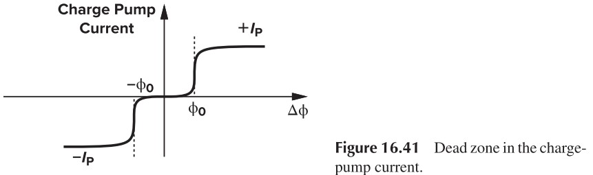
The dead zone will cause jitter as it allow the VCO to accumulate as much random phase error as $\phi_0$.
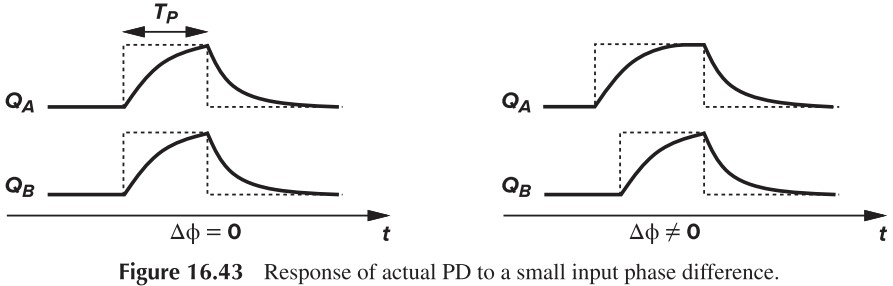
有趣的是,这个 Nonideal effect 被另一个 Nonideal effect 解决了。由于 $Q_A,Q_B$ activate the reset 也需要一定时间,这就会导致即使在 zero phase 时,PFD 会输出一个很小的 pulse $T_P$(Fig. 16.39),若这个 $T_P$ 刚好打开 CP,就能消除死区(Fig. 16.43)
Delay Difference Between $Q_A$ and $Q_B$ 简而言之就是 由于 $Q_A$ 经过了一个反相,会滞后于 $Q_B$,解决方法就是在 $Q_B$ 上加一个传输门(Fig. 16.44)
%20Implementation%20of%20charge%20pump;%20(b)%20effect%20of%20skew%20between%20QA%20and%20QB;%20(c)%20suppression%20of%20skew%20by%20a%20pass%20gate.jpg)
The Mismatch Between The Drain Currents of $M_1$ and $M_2$(充、放电电流失配),这会导致 $V_\tx{cont}$ 在 $\Delta phi=0$ 时不能保持恒定(Fig. 16.45a)。在存在某个特殊的相位差时,Net Current=0,此时 $V_\tx{cont}$ 才能恒定(但实际还是有波纹)。
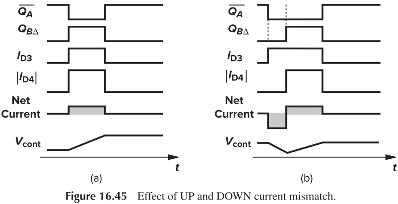
充、放电电流失配的原因主要是沟道长度调制效应,因此可以利用“反馈”来调整 gate 的电压,从而使电流相同。
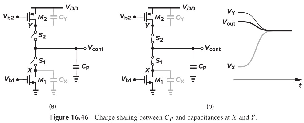
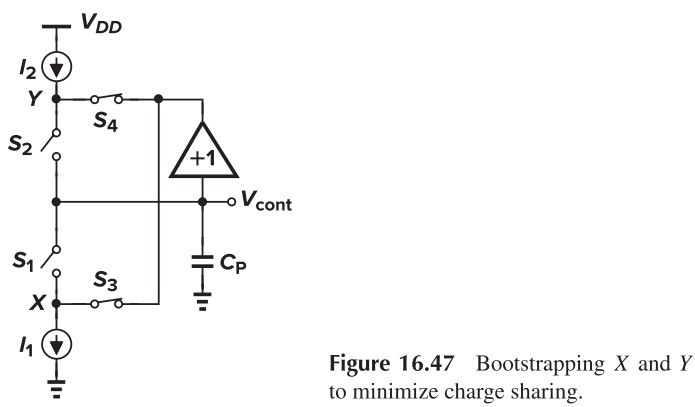
Charge-Sharing Phenomenon 由于 MOS 存在电容,所以在开关打开时,电荷会在电容之间平分,导致 Vcont 电压下降(Fig. 16.46),解决方法很简单,添加 bootstrapping 来给电容预充电。