Common-Gate Stage

Fig 3.48(a) 可以转换成 Fig 3.48(b)。We first study the large-signal behavior.
- $V_b-V_\tx{in}<V_\tx{TH}$, $M_1$ is off, $V_\tx{out}=V_{DD}$
- $V_b-V_\tx{in}>V_\tx{TH}$, $M_1$ is in saturation, $I_D$ is
and $V_\tx{out}$ is
\[V_\tx{out}=V_{DD} - I_D R_D\]we can obtain a small-signal gain of
\[\begin{aligned} \frac{\p V_\tx{out}}{\p V_\tx{in}}&=-R_D \frac{\p I_D}{\p V_\tx{in}}\\ &=-R_D \mu_n C_\tx{ox} \frac{W}{L}(V_b-V_\tx{in}-V_\tx{TH}) \\ &\quad (-1-\frac{\p V_\tx{TH}}{\p V_\tx{in}})\\ \tx{with }&\frac{\p V_\tx{TH}}{\p V_\tx{in}}=\frac{\p V_\tx{TH}}{\p V_{SB}}=\eta\\ \frac{\p V_\tx{out}}{\p V_\tx{in}}&=g_m(1+\eta)R_D \end{aligned}\]$\eta$ 是那个体效应的参数,所以和 $\p V_{TH}$ 有关。注意到 $\eta$ 的存在增大了增益。
回到 large-signal behavior,我们还漏了一种情况没说,即
- $V_b-V_\tx{TH}>V_\tx{out}$, $M_1$ is in triode region
我们将三种情况总结为下图 Fig. 3.49

The small-signal equivalent circuit of CG stage is

下面计算小信号增益:
\[r_O(\frac{-V_\tx{out}}{R_D}-g_m V_1 - g_{mb}V_1) - \frac{V_\tx{out}}{R_D}R_S+V_\tx{in} = V_\tx{out}\\ \tx{where } V_1 - \frac{V_\tx{out}}{R_D}R_S+V_\tx{in}=0\\ \Downarrow\\ A_v=\frac{V_\tx{out}}{V_\tx{in}}=\frac{(g_m+g_{mb})r_O+1}{r_O+(g_m+g_{mb})r_OR_S+R_S+R_D}R_D\\ =\frac{[1+(g_m+g_{mb})r_O]R_D}{r_O+[1+(g_m+g_{mb})r_O]R_S+R_D}\]注意到 $[1+(g_m+g_{mb})r_O]$ 和之前 CS stage 的 degenerated factor 是一样的。利用这个我们可以很快地把这个公式记下来。
下面计算输入&输出阻抗:

注意:这里没有考虑 $R_S$
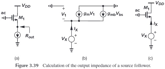
如果 $R_D=0$,就和之前 source follower(Fig. 3.39a)的输出是一样的(老实说,书上这样讲不是很好,应该说“如果忽略 $r_O$,那么从源端看进去的电阻就是 $\dfrac{1}{g_m}\Vert\dfrac{1}{g_{mb}}$”,这样的话就能将 diode-conneted 的情况也包含进去,见下表的总结)。
| 从源端看进去的电阻 | diode-conneted | source follower | CG stage |
|---|---|---|---|
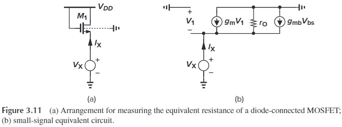 |
 |
|
|
| 无 $r_O$ | $\dfrac{1}{g_m}\Vert\dfrac{1}{g_{mb}}$ | $\dfrac{1}{g_m}\Vert\dfrac{1}{g_{mb}}$ | $\dfrac{1}{g_m}\Vert\dfrac{1}{g_{mb}}$ |
| 有 $r_O$ | $\dfrac{1}{g_m+g_{mb}+1/r_O}$ | $\dfrac{1}{g_m+g_{mb}+1/r_O}$ | $\dfrac{R_D/r_O+1}{g_m+g_{mb}+1/r_O}$ |
至于输出电阻,就和之前 source degeration 是一样的(见 Fig. 3.57)。我们可以直接写出:
\[R_\tx{out}=\left\{ [1+(g_m+g_{mb})r_O]R_S+r_O \right\} \Vert R_D\\ 或=\left\{ [1+(g_m+g_{mb})R_S]r_O+R_S \right\} \Vert R_D\]
总结
个人感觉 Common-gate 是三种 Stage 中最难记的,因为我们很难用之前的直接去概括它。我个人是这样想的:
- $R_\tx{out}=\left\{ [1+(g_m+g_{mb})r_O]R_S+r_O \right\} \Vert R_D$ 和 Common-source 一样,这个简单
- $R_\tx{in}=\dfrac{R_D+r_O}{1+(g_m+g_{mb})r_O}$,前面的 Degenerated Factor 是乘以 $R_S$,这里恰好相反(注意,这里没有考虑 $R_S$,实际要加上 $R_S$)
- $A_v=\dfrac{(g_m+g_{mb})r_O+1}{r_O+(g_m+g_{mb})r_OR_S+R_S+R_D}R_D$,分母是所以电阻串联(且 $R_S$ 乘上 Degenerated Factor),而分母是 Degenerated Factor 乘上 $R_D$
关于增益,我们可以改写为:
\[\begin{aligned} A_v &= \frac{R_D}{R_S+\dfrac{(R_D+r_O)}{1+(g_m+g_{mb})r_O}}\\ &=\frac{i \cdot R_{D}}{i\cdot R_{\tx{in}}}\\ &=\frac{V_\tx{out}}{V_\tx{in}} \end{aligned}\]分母是输入端往上看到的电阻,分母是输出端的 $R_D$。它们分别乘上电流后,就是输入和输出电压!这样就好理解了!