Single-Ended and Differential
- Single-End: 相对于固定电势(一般是地)
- Differential: 相对于一个相反的信号
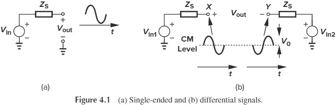
An important advantage of differential operation over single-ended signaling is higher immunity to“environmental” noise. Assume
\[V_1 = V+\Delta V\\ V_2 = -V+\Delta V\]The differential signal of $V_1$ and $V_2$ is
\[V_1-V_2=2V\]which cancels the noise $\Delta V$
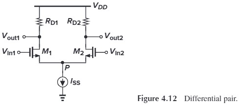
Basic Differential Pair
Here, two differential inputs, $V_\tx{in1}$ and $V_\tx{in2}$, having a certain CM (common mode) level, $V_\tx{in,CM}=\dfrac{V_\tx{in1}+V_\tx{in2}}{2}$. The output also have $V_\tx{out,CM}$
if we use two independent cs stage amplifier, a low $V_\tx{in,CM}$ may lead to clipping at the output. (Why?) Therefore, we use the circuit below:
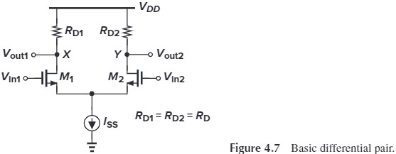
下面我们先考虑一些总体的特性:
- $I_{SS}=I_{D1}+I_{D2}$ is independent of $V_\tx{in,CM}$.
- If $V_\tx{in1}=V_\tx{in2}$, the output CM level is $V_{DD}-R_DI_{SS}/2$.
- $V_\tx{out1}$ reaches its minimum value $V_{DD}-R_DI_{SS}$ when $V_\tx{out2}$ is at its maximum value $V_{DD}$, therefore the maximum differential output is $\pm R_DI_{SS}$
上面三点即下图:
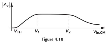
下面我们考虑工作在各个工作区的情况(Fig. 4.9):
- $V_\tx{in,CM}=0$, $M_1,M_2$ is off, $I_{D3}=0$, $M_3$ operates in the deep triode region ($V_b>V_\tx{TH}$,and $V_{S}=V_{D}=0$)
- $V_\tx{in,CM}\geq V_\tx{TH}$, $M_1,M_2$ is on, $V_P$ also rise. In a sense, $M_1,M_2$ constitute a source follow, $V_P$ follows $V_\tx{in,CM}$(此时 $M_3$ 可看作电阻)
- $V_\tx{in,CM}>V_{GS1}+V_{GS3}-V_\tx{TH3}$, i.e. $V_P>V_{GS3}-V_\tx{TH3}$, $M_3$ operate in saturation, 即 Fig 4.7,$I_{D1,2}$ reaches maximum
- $V_\tx{in,CM}>V_\tx{out1,max}+V_\tx{TH}=V_{DD}-R_DI_{SS}/2+V_\tx{TH}$, $V_\tx{out}$ remains its minimum.
综上,我们希望 $V_\tx{in,CM}$ 在 3. 的范围,即:
\[V_{GS1}+(V_{GS3}-V_\tx{TH3}) \leq V_\tx{in,CM} \leq \min \left\{ V_{DD}-R_DI_{SS}/2+V_\tx{TH}, V_{DD} \right\}\]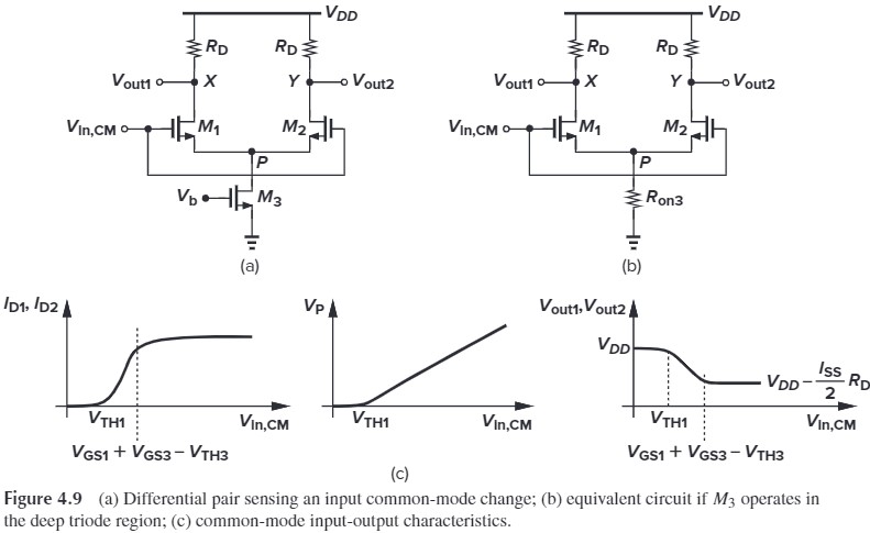
对 $I_{D1,2}$ 微分就能得到 $\vert A_v \vert$ 随共模电平的变化曲线。
Quantitative Analysis
Large-Signal Behavior
下面我们来推导 $V_\tx{out1}-V_\tx{out2}$ 与 $V_\tx{in1}-V_\tx{in2}$ 的关系。
首先,
\[\begin{aligned} &V_\tx{out1}-V_\tx{out2}\\ =& (V_{DD}-R_{D1}I_{D1})-(V_{DD}-R_{D2}I_{D2})\\ =& R_{D2}I_{D2}-R_{D1}I_{D1}\\ =& R_D(I_{D2}-I_{D1}) \quad \tx{if} R_{D1}=R_{D2}=R_D \end{aligned}\] \[\begin{aligned} &V_\tx{in1}-V_\tx{in2}\\ &= (V_{GS1}+V_P)-(V_{GS2}+V_P)\\ &= V_{GS1}-V_{GS2} \end{aligned}\]所以我们只需要求 $I_{D2}-I_{D1}$ 与 $V_{GS1}-V_{GS2}$ 的关系。之前我们求过 $I_D$ 与 $V_{GS}$ 有如下关系:
\[I_D = \frac{1}{2} \mu_n C_\tx{ox} \frac{W}{L} (V_{GS}-V_\tx{TH})^2\]由于右边有平方,所以直觉告诉我们要开方:
\[\sqrt{\frac{I_D}{\frac{1}{2} \mu_n C_\tx{ox} \frac{W}{L}}} = V_{GS}-V_\tx{TH}\]所以 $V_{GS1}-V_{GS2}$ 为:
\[\begin{aligned} V_{GS1}-V_{GS2} &= \sqrt{\frac{I_{D1}}{\frac{1}{2} \mu_n C_\tx{ox} \frac{W}{L}}} - \sqrt{\frac{I_{D2}}{\frac{1}{2} \mu_n C_\tx{ox} \frac{W}{L}}} \end{aligned}\]两边平方后:
\[\begin{aligned} (V_{GS1}-V_{GS2})^2 &= \frac{2}{\mu_n C_\tx{ox} \frac{W}{L}} (I_{D1}-2\sqrt{I_{D1}I_{D2}}+I_{D2})\\ &= \frac{2}{\mu_n C_\tx{ox} \frac{W}{L}} (I_{SS}-2\sqrt{I_{D1}I_{D2}}) \end{aligned}\\ -2 \sqrt{I_{D1}I_{D2}} = \frac{1}{2} \mu_n C_\tx{ox} \frac{W}{L}(V_{GS1}-V_{GS2})^2-I_{SS}\]为了得到 $I_{D1}-I_{D2}$,我们需要利用下式:
\[4I_{D1}I_{D2}=(I_{D1}+I_{D2})^2-(I_{D1}-I_{D2})^2=I_{SS}^2-(I_{D1}-I_{D2})^2\]从而(这里还将 $V_{GS}$ 换成了 $V_\tx{in}$):
\[\left[ \frac{1}{2} \mu_n C_\tx{ox} \frac{W}{L}(V_\tx{in1}-V_\tx{in2})^2-I_{SS} \right]^2=I_{SS}^2-(I_{D1}-I_{D2})^2\]将左边展开再进行一定的化简后,有:
\[I_{D1}-I_{D2} = \frac{1}{2} \mu_n C_\tx{ox} \frac{W}{L}(V_\tx{in1}-V_\tx{in2})\sqrt{\frac{4I_{SS}}{\mu_n C_\tx{ox}\frac{W}{L}}-(V_\tx{in1}-V_\tx{in2})^2}\]总的来看,这个单调递增的奇函数。我们可以求斜率:
\[G_m = \frac{\p \Delta I_D}{\p \Delta V_\tx{in}}=\frac{1}{2} \mu_n C_\tx{ox} \frac{W}{L} \frac{\dfrac{4I_{SS}}{\mu_n C_\tx{ox}\frac{W}{L}}-2\Delta V_\tx{in}^2}{\sqrt{\dfrac{4I_{SS}}{\mu_n C_\tx{ox}\frac{W}{L}}-\Delta V_\tx{in}^2}}\]易看出 $\Delta V_\tx{in}^2$越小,$G_m$ 越大。所以在 $\Delta V_\tx{in}=0$ 处 $G_m$ 取最大值 $\sqrt{\mu_n C_\tx{ox}\frac{W}{L}I_{SS}}$,对应的增益为:
\[\vert A_v \vert = \sqrt{\mu_n C_\tx{ox}\frac{W}{L}I_{SS}} \cdot R_D\]注意到每个 MOS 的 $I_D=\dfrac{1}{2}I_{SS}$,所以上面 $\vert A_v \vert$ 的表达式实际上和之前 CS Stage 是一样的,都是 $g_m R_D$。(这里英语书上 108 页认为 $\Delta V_\tx{out}=R_D \Delta I = -R_D G_m \Delta V_\tx{in}$,但根据上面 $G_m$ 的定义式,不应该有负号的。建议去问问老师)
另一方面,当 $\vert \Delta V_\tx{in} \vert=\sqrt{\frac{2I_{SS}}{\mu_n C_\tx{ox} \frac{W}{L}}}$ 时,$G_m=0$.
如果我们继续增大 $\vert \Delta V_\tx{in} \vert$ 到 $\sqrt{\frac{4I_{SS}}{\mu_n C_\tx{ox} \frac{W}{L}}}$,分母中的根号部分就等于零,使得 $G_m$ 趋向于无穷。但看回 Fig. 4.8,曲线并没有趋向于无穷。为什么呢?
书上说是因为当 $\Delta V_\tx{in}$ 大到一定程度时(我们记为 $\Delta V_\tx{in1}$),其中一只管子会先达到 triode region,使得 $I_{SS}$ 全部都流经它,导致另一个管子 off. 我们可以计算一下此时的 $\Delta V_\tx{in}$。首先,$M_2$ is nearly off, $V_{GS2}=V_\tx{TH}$, 故
\[\Delta V_\tx{in1}=V_{GS}-V_\tx{TH}\]又因为 $I_{D1}=I_{SS}$,所以我们有:
\[I_{SS}=\frac{1}{2}\mu_n C_\tx{ox} \frac{W}{L} \Delta V_\tx{in}^2\\ \Rightarrow \Delta V_\tx{in1} = \sqrt{\dfrac{2 I_{SS}}{\mu_n C_\tx{ox} \frac{W}{L}}}\]因为此时的 $V_\tx{out1}$ 固定为 $I_{SS}R_{D1}$,$V_\tx{out2}=0$,所以小信号增益为 0,即 $G_m=0$。最终我们可以画出完整的 $G_m-V_\tx{in}$ 关系图:
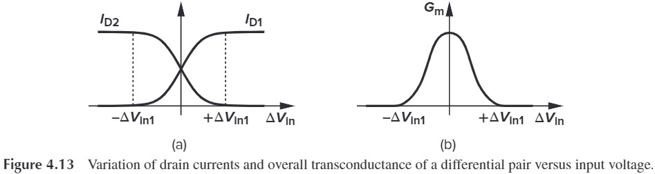
$\Delta V_\tx{in1}$ is the maximum differential input, and for zero differential input, $I_{D1}=I_{D2}=I_{SS}/2$, yielding
\[(V_{GS}-V_\tx{TH})_{1,2}=\sqrt{\dfrac{I_{SS}}{\mu_n C_\tx{ox}\frac{W}{L}}}\]Thus, $\Delta V_\tx{in1}$ is equial to $\sqrt{2}$ times the equilibrium overdrive.
Small-Signal Analysis
下面我们将用小信号的方法得到上面的结果:
\[\begin{aligned} \vert A_v \vert &= \sqrt{\mu_n C_\tx{ox} I_{SS} W/L} \cdot R_D\\ &= g_m R_D \end{aligned}\]Method 1
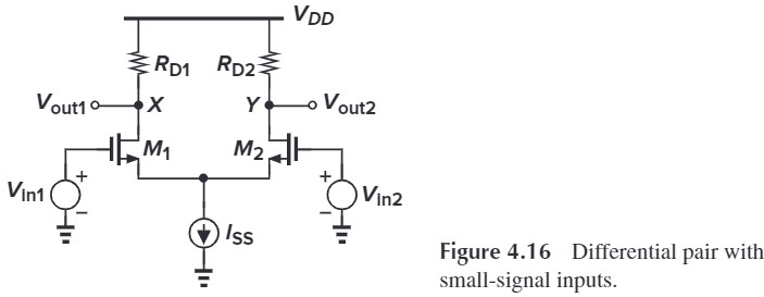
superposion (叠加定理): The circuit of Fig. 4.16 is driven by two independent signals.
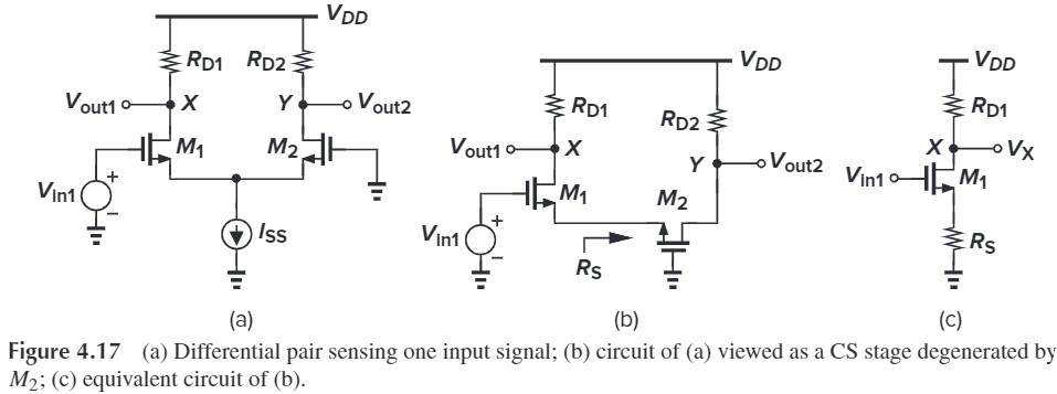
First, let’s set $V_\tx{in2}$ to zero, and only calculate the effect of $V_\tx{in1}$ at $X$ and $Y$.
To calculate $V_X$: the impedance seen looking into the source of $M_2$ is $R_s=1/g_{m2}$, therefore $M_1$ forms a common-source stage with a degeneration resistance (Fig. 4.17a), and
\[\frac{V_X}{V_\tx{in1}} = \frac{-R_D}{\dfrac{1}{g_{m1}}+\dfrac{1}{g_{m2}}} \tag{4.18}\]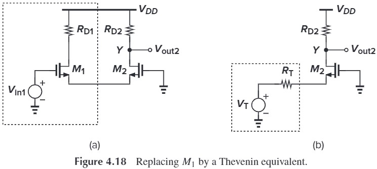
To calculate $V_Y$: replace $V_\tx{in1}$ and $M_1$ by Thevenin equivalent (Fig. 4.18), the Thevenin voltage $V_T = V_\tx{in1}$ and the resistance $R_T=1/g_m$, therefore $M_2$ operates as a common-gate stage, and
\[\frac{V_Y}{V_\tx{in1}}=\frac{R_D}{\dfrac{1}{g_{m1}}+\dfrac{1}{g_{m2}}} \tag{4.19}\]The overall voltage gain for $V_\tx{in1}$ is
\[(V_X-V_Y)\Big\vert_\tx{Due to Vin1} = \frac{-2R_D}{\dfrac{1}{g_{m1}}+\dfrac{1}{g_{m2}}} V_\tx{in1} \tag{4.20}\]which, for $g_{m1}=g_{m2}=g_m$, reduces to
\[(V_X-V_Y)\Big\vert_\tx{Due to Vin1} = -g_m R_D V_\tx{in1} \tag{4.21}\]By virue of symmetry, the voltage gain for $V_\tx{in2}$ is identical to that of $V_\tx{in1}$ except for a change in the polarities:
\[(V_X-V_Y)\Big\vert_\tx{Due to Vin2} = g_m R_D V_\tx{in2} \tag{4.22}\]Adding $(4.21)$ and $(4.22)$, we have
\[\frac{(V_X-V_Y)}{V_\tx{in1}-V_\tx{in2}}=-g_m R_D\]Method 2
下面我们将介绍一种叫 半边电路 half circuit 的方法,这种方法适用于对称的差分放大器。首先先介绍一个定理:
Consider the symmetrc circuit shown in Fig. 4.20. 如果 $V_\tx{in1}$ 和 $V_\tx{in2}$ 变化幅度相反(电路保持线性性),那么 $V_p$ 不变。

证明:从直觉上来说这里是正确的,但我们依然严格证明一下。假设 $V_{1,2}$ 从 $V_a$ 变化为:
$$
V_1 = V_a+ \Delta V_1\\
V_2 = V_a- \Delta V_2
$$
那么电流的变化量为:
$$
\Delta I_1 = g_m \Delta V_1\\
\Delta I_2 = -g_m \Delta V_2
$$
由于 $I_1+I_2=I_T$,所以:
$$
\Delta I_1 +\Delta I_2=0\\
\Rightarrow \Delta V_1=\Delta V_2
$$
注意到:$V_\tx{in1}-V_1=V_\tx{in2}-V_2=V_P$,对两边取微分 $\Delta V_\tx{in}-\Delta V_1=-\Delta V_\tx{in}+\Delta V_2$,整理得:$\Delta V_\tx{in}=\Delta V_1=\Delta V_2$
那么 $P$ 处的电压为:
$$
\begin{aligned}
V_P&=V_\tx{in1}-V_1\\
&=(V_0+\Delta V_\tx{in}) - (V_a+\Delta V_1)\\
&=V_0-V_a\\
&或\\
&=V_\tx{in2}-V_2\\
&=(V_0-\Delta V_\tx{in}) - (V_a-\Delta V_2)\\
&=V_0-V_a
\end{aligned}
$$
得证。
既然 $V_P$ 保持不变,那么在小信号模型中就相当于地,所以我们有 Fig 4.22b
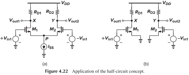
这么一来,就可以直接用之前 CS stage 的结论对半边电路求解,从而 $(V_X-V_Y)/(2V_\tx{in1})=-g_m R_D$. 这种方法又快又简单,推荐凡是电路对称的都使用这种方法;但如果电路不对称(比如要求 CMRR 时),就只能用前一种方法。
Degenerated Differential Pair
与 common-source stage 类似,differential pair 可以通过增加 resistive degeneration 来增加线性性(Fig. 4.27)。我们可以用公式来证明这一点。
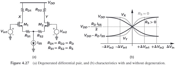
假设当 $V_\tx{in1}-V_\tx{in2}$ 达到某个值 $\Delta V_\tx{in2}$ 时,$M_2$ 断开而 $I_{D1}=I_{SS}$,此时:
\[V_\tx{in1}-V_{GS1}-R_S I_{SS} = V_\tx{in2}-V_\tx{TH}\\ \begin{aligned} \Rightarrow V_\tx{in1}-V_\tx{in2} &= V_{GS1}-V_\tx{TH}+R_SI_{SS}\\ &= \sqrt{\frac{2 I_{SS}}{\mu_n C_\tx{ox} (W/L)}} + R_S I_{SS} \end{aligned}\]注意到第一项就是 $\Delta V_\tx{in1}$,说明 $\Delta V_\tx{in2}$ 比 $\Delta V_\tx{in1}$ 大 $R_S I_{SS}$,也就是说,线性区增大了约 $\pm R_S I_{SS}$
而增益就是加上了 $R_S$:
\[\vert A_v \vert = \frac{R_D}{\frac{1}{g_m} + R_S}\]The circuit thus trades gain for linearity—as is also observed from the slopes of the characteristics in Fig. 4.27(b)
Common-Mode Response
由于电路不可能完全对称,并且不存在阻抗无穷大的电流源,所以 a fraction of the input CM variation appears at the output.
先假设电路对称,但电流源的阻值为 $R_{SS}$,我们可以利用对称性将 Fig. 4.29(a) 简化为 (c)
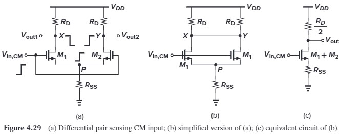
从而共模增益为(貌似这个也是差模增益):
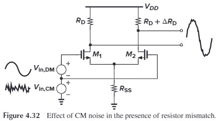
\[\begin{aligned} A_{v,\tx{CM}} &= \frac{V_\tx{out}}{V_{in,\tx{CM}}}\\ &= - \frac{R_D/2}{1/(2g_m)+R_{SS}} \end{aligned}\]当然,这没什么好担心的,因为我们的输出是差模输出,但假如电路不对称的话,情况就不一样了。假如两个 $R_{D}$ 不匹配 Fig. 4.31(称为 resisor mismatch),那么,我们有:
\[\begin{aligned} \Delta V_X &= -\Delta V_{in,\tx{CM}} \frac{g_m}{1+2g_mR_{SS}} R_D\\ \Delta V_Y &= -\Delta V_{in,\tx{CM}} \frac{g_m}{1+2g_mR_{SS}} (R_D+\Delta R_D) \end{aligned}\]这就会导致差模输出中含有输入的共模噪声。
另一种 mismatch 是 $M_1,M_2$ 不匹配。我们考虑下图 Fig. 4.34
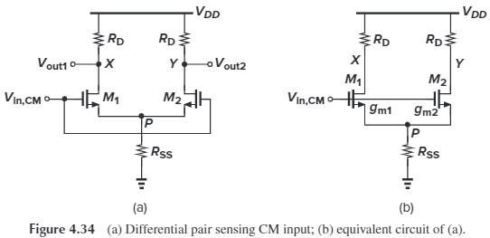
根据:
\[\begin{aligned} (I_{D1}+I_{D2})R_{SS}&=V_P\\ (g_{m1}+g_{m2})(V_\tx{in,CM}-V_P)R_{SS} &= V_P \end{aligned}\]我们有:
\[V_P = \frac{(g_{m1}+g_{m2})R_{SS}}{(g_{m1}+g_{m2})R_{SS}+1} V_\tx{in,CM}\]从而输出电压分别为:
\[\begin{aligned} V_X &= -g_{m1} (V_\tx{in,CM}-V_P)R_D\\ &= \frac{-g_{m1}}{(g_{m1}+g_{m2})R_{SS}+1} R_D V_\tx{in,CM} \end{aligned}\] \[\begin{aligned} V_Y &= -g_{m2} (V_\tx{in,CM}-V_P)R_D\\ &= \frac{-g_{m2}}{(g_{m1}+g_{m2})R_{SS}+1} R_D V_\tx{in,CM} \end{aligned}\]所以我们可得共模转差模的增益为:
\[\begin{aligned} A_\tx{CM-DM} &= \frac{V_X-V_Y}{V_\tx{in,CM}}\\ &= -\frac{\Delta g_m R_D}{(g_{m1}+g_{m2})R_{SS}+1} \end{aligned}\]我们定义 共模抑制比 common-mode rejection ratio(CMRR) 为:
\[\tx{CMRR} = \left\vert \frac{A_\tx{DM}}{A_\tx{CM-DM}} \right\vert\]显然,共模抑制比越大越好。理想情况应该为无穷大。
利用 Fig 4.17 可以证明,当 $g_m$ mismatch 时,差模增益为:
\[\begin{aligned} \vert A_\tx{DM} \vert &= \frac{R_D/2}{\dfrac{1}{g_{m1}+g_{m2}}+R_{SS}}+\frac{2g_{m1}g_{m2}R_D}{\dfrac{1}{R_{SS}}+g_{m1}+g_{m2}}\\ &= \frac{R_D}{2} \left( \frac{g_{m1}+g_{m2}+4g_{m1}g_{m2}R_{SS}}{1+(g_{m1}+g_{m2})R_{SS}} \right) \end{aligned}\]注意到第一项和 Fig. 4.29 的共模增益是类似的,而第二项和 Fig. 4.17 的差模增益是类似的。这是为什么?
从而 CMRR 为:
\[\begin{aligned} \tx{CMRR} &= \frac{g_{m1}+g_{m2}+4g_{m1}g_{m2}R_{SS}}{2 \Delta g_{m}}\\ &\approx \frac{g_m}{\Delta g_m}(1+2g_m R_{SS}) \end{aligned}\\ 此处 g_m = \frac{g_{m1}+g_{m2}}{2}\]由于 $2g_m R_{SS} \gg 1$,所以可以进一步化简得到 $\tx{CMRR}\approx 2 g_m^2 R_{SS}/\Delta g_{m}$