General Considerations
In summary, if a negative-feedback circuit has a loop gain that satisfies two conditions:
\[\begin{aligned} \vert H(j\omega_0) \vert &\geq 1\\ \angle H(j\omega_0) &= 180^\circ \end{aligned}\]For the oscillation to begin, a loop gain of unity or greater is necessary.
Ring Oscilators
A ring oscillator consists of a number of gain stages in a loop. We start from single-stage feedback to multi-stage feedback.
电路一

From Fig. 15.4, the open-loop circuit contains only one pole, thereby providing a maximum frequency dependent phase shift of $90^\circ$ (at a frequency of infinity). Added by a dc phase shift of $180^\circ$, the max total phase shift is $270^\circ< 360^\circ$. The loop therefore fails to sustain oscillation growth.
电路二

- two pole → $180^\circ$
- dc phase shift → $360^\circ$
电路三

- dc phase shift → $540^\circ$
- two pole → $180^\circ$
电路四

- dc phase shift → $540^\circ$
- two pole → $270^\circ$
从上面几个案例,我们可以总结如下分析步骤:
- 判断 dc phase shift
- 判断 pole 带来的 phase shift
- 把 1 和 2 相加,看在 $(0,\infty)$ 内 total phase shift 能否够 360 (并且 360 时不能在 0 或 $\infty$)
- 判断在 360 时 gain 是否大于等于 1

下面我们继续分析最后一个 3 级振荡器,我们还需要考虑增益。设每一级的传输函数为 $\dfrac{-A_0}{1+s/\omega_0}$,则 loop gain 为:
\[H(s) = -\frac{A_0^3}{(1+\dfrac{s}{\omega_0})^3}\]要使相移达到 $180^\circ$,则每一级贡献 $60^\circ$,即:
\[\arctan \frac{\omega_\tx{osc}}{\omega_0} = 60^\circ\\ \Rightarrow \omega_\tx{osc} = \sqrt{3} \omega_0\]代入 loop gain,得到:
\[\frac{A_0^3}{\left[\sqrt{1+(\dfrac{\omega_\tx{osc}}{\omega_0})}\right]^3} = 1\\ \Rightarrow A_0 = 2\]总结, a three-stage ring oscillator requires a low-frequency gain of 2 per stage, and it oscillates at a frequency of $\sqrt{3} \omega_0$, where $ω_0$ is the 3-dB bandwidth of each stage
LC Oscillators
Basic
我们先来回顾一下电路与高频的知识。
对于 LC 并联电路,我们有:
\[Z = \frac{1}{j\omega C+\dfrac{1}{j\omega L}}\]当 $j\omega C = \dfrac{1}{j\omega L}$,即 $\omega = 1/\sqrt{LC}$ 时,$Z=\infty$,此时为谐振状态(电路的知识)
考虑上电感的电阻

对于 Fig. 15.21a,
\[Z = \frac{(R + j \omega L) \frac{1}{j\omega C} }{ R + j(\omega L - \frac{1}{\omega C})}\]当 $\omega = 1/\sqrt{LC}$ 时,$Z$ 达到最大值 $\dfrac{L}{CR}$。完整的幅频特性如下图所示:
%20Magnitude%20and%20(b)%20phase%20ofthe%20impedance%20ofan%20LC%20tank%20as%20a%20function%20of%20frequency.jpg "Figure 15.22 (a) Magnitude and (b) phase ofthe impedance ofan LC tank as a function of frequency")
有时候我们希望电阻也是并联的,这样好算一点。转换的方法如下(具体推导过程略)
\[C_p=C_1\\ L_p=L_1\\ R_p \approx \frac{L_1^2 \omega^2}{R_S} =Q^2 R_S\\\]转换成并联后,我们可以写出其 $Q$ 值为 $Q_p = \dfrac{R_p}{\omega_p L}=R_p \omega_p C= R_p \sqrt{\dfrac{C}{L}}$
Cross-Coupled Oscillator
我们将 LCR 振荡网络作为负载。当只有一级时,CS 贡献 $180^\circ$,RLC 贡献 $-90^\circ\sim 90^\circ$,加起来不够 $360^\circ$
%20Tuned%20gain%20stage;%20(b)%20stage%20of%20(a)%20in%20feedback.jpg)
如果再增加一级,CS 贡献 $360^\circ$,RLC 贡献 $-180^\circ\sim 180^\circ$,那么在谐振频率处刚好是 $360^\circ$,可以起振。注意对比之前 2 级反相的情况,由于之前的 0 相移在 DC,所以被锁定,无法振荡。
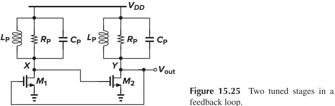
我们从另一个角度来理解为什么上面这种解法可以振荡。我们将电路整理一下就会发现,下面两个MOS组成了负阻(前面某道练习题有说),负阻抵消了振荡的电阻损耗,使得振荡可以维持下去。
%20Redrawing%20of%20the%20oscillator%20shown%20in%20Fig.%2015.25;%20(b)%20another%20redrawing%20of%20the%20circuit;%20(c)%20addition%20of%20tail%20current%20source%20to%20lower%20supply%20sensitivity.jpg)
下面我们来详细研究一下这个负阻结构。
%20Source%20follower%20with%20positive%20feedback%20to%20create%20negative%20input%20impedance;%20(b)%20equivalent%20circuit%20of%20(a)%20to%20calculate%20the%20input%20impedance.jpg "Figure 15.33 (a) Source follower with positive feedback to create negative input impedance; (b) equivalent circuit of (a) to calculate the input impedance")
考虑 Fig. 15.33b 的小信号模型,有:
\[\begin{cases} V_X - V_1 + V_2 = 0\\ I_X = g_{m2}V_2 = - g_{m1}V_1 \end{cases}\\ \Rightarrow V_X + \frac{I_X}{g_{m1}} + \frac{I_X}{g_{m2}} = 0\\ \Rightarrow \frac{V_X}{I_X} = -\frac{1}{1/g_{m1}+1/g_{m2}}\]若 $g_{m1}=g_{m2}=g_m$,则这个电路具有一个负阻 $-\dfrac{2}{g_m}$。
要让 $-\dfrac{2}{g_m}$ 抵消两个 $R_P$,则 $g_m = \frac{1}{R_P}$,此时的差分增益为 $g_m R_P = 1$,这也是差分增益的最小要求。
另一种负阻结构如下图所示:
%20Circuit%20topology%20providing%20negative%20resistance;%20(b)%20equivalent%20circuit%20of%20(a);%20(c)%20oscillator%20using%20(a).jpg)
根据小信号模型容易写出:
\[V_X = (I_X - \frac{-I_X}{C_1 s}g_m) \frac{1}{C_2 s}+\frac{I_X}{C_1 s}\\ \Rightarrow \frac{V_X}{I_X}=\frac{g_m}{C_1 C_2 s^2}+\frac{1}{C_2 s}+\frac{1}{C_1 s}\]注意到第一项是负的($s^2=-\omega^2$),所以 Fig. 15.17c 的结构是可以振荡的。
Colpitts Oscillator
%20Colpitts%20oscillator;%20(b)%20equivalent%20circuit%20of%20(a)%20with%20input%20stimulus.jpg)
详细分析看书,我这里只是简单说一下。首先我们需要把这个看作一个 CG Stage,输出的电压经过电容分压后再放大 $g_m R_D$ 倍(忽略 $g_{mb}$),以弥补 $R_P$ 的损耗。其振荡频率为:
\[\omega_R^2 = \frac{1}{L_P C}\\ C=\frac{1}{1/C_1+1/C_2}\]而放大倍数需要满足:
\[g_m R_P = \frac{(C_1+C_2)^2}{C_1C_2}\]关于这个式子的来源嘛,书上列举了一大堆公式,你可以去看一下。我们一般把这个表示为 $\frac{C_1}{C_2}$ 的函数,即:
\[g_m R_P = \frac{C_1}{C_2}(1+\frac{C_2}{C_1})^2 \geq 4\\\]最小值可以在 $\frac{C_1}{C_2} = 1$ 时取得.
相关论文:Output voltage analysis for the MOS Colpitts oscillator
Voltage-Controlled Oscillators
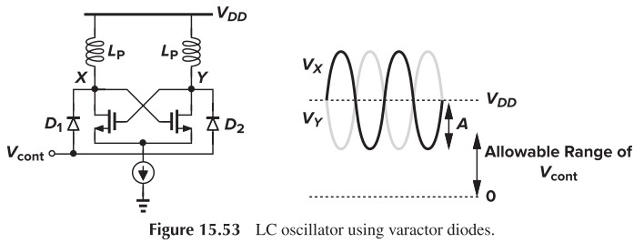
现在我们想要让电压能控制频率,而要改变谐振频率,则必须改变 L 或 C,由于电感很难改变,所以我们必须用0可变电容。在半导体器件中,我们知道二极管两边的反偏电容会随着电压改变,即:
\[C_\tx{var} = \frac{C_0}{(1+\dfrac{V_R}{\phi_B})^m}\]电路图见 Fig. 15.53
对于 Ring Oscillators,对于 N 个反相器组成的延时电路,其振荡频率是 $(2NT_D)^{-1}$。我们可以通过改变反相器的延时时间来改变周期,具体电路如下:
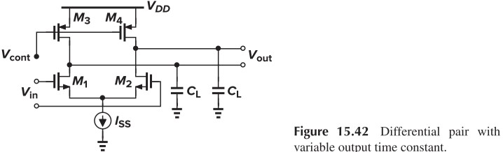
其中,M3、M4 处于深度线性区,对应的 RC 延时为:
\[\begin{aligned} \tau &= R_{3,4} C_L\\ &=\frac{C_L}{\mu_p C_\tx{ox} (\frac{W}{L})_{3,4}(V_{DD}-V_\tx{cont}-\vert V_\tx{THP}\vert)} \end{aligned}\]Mathematical Model of VCOs
我们知道,相位是频率的积分,频率是相位的微分(就像速度和路程一样),那么,当频率变快时,相位的积累速度就会变快。可以参考下面这幅图:
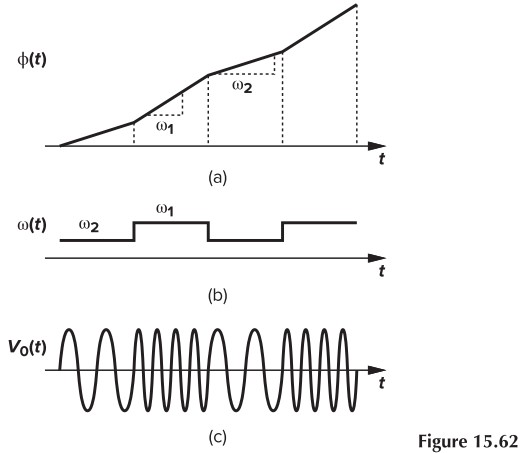
用公式表述如下:
\[\begin{cases} \phi = \int \omega \dif t + \phi_0\\ \omega_\tx{out}=\omega_0 + K_{VCO}V_\tx{cont} \end{cases}\] \[\begin{aligned} V_\tx{out}(t) &= V_m \cos\left( \int \omega_\tx{out} + \phi_0 \right)\\ &=V_m \cos (\omega_0 t+K_{VCO}\int V_\tx{cout} \dif t+\phi_0) \end{aligned}\\ \Rightarrow\phi_{ex} = K_{VCO} \int V_\tx{cont} \dif t\\ \Rightarrow\frac{\phi_{ex}}{V_\tx{cont}}(s) = \frac{K_{VCO}}{s}\]从公式中可以看出,VCO 实际上是一个积分器!为什么要说这个呢?因为后续我们可能需要对系统进行建模,需要求出系统函数(也就是信号与系统中学的拉普拉斯变换啦!忘了的同学可以去看本站的相关笔记)。