Basic Idea of Reference
集成电路中会用到很多基准电压,比如:
- Supply-independent biasing
- Proportional to absolute temperature (PTAT) reference
- Constant-Gm behavior reference
- Temperature independent reference
为啥要这么多基准呢?理想情况下,我们希望基准电压(1)不受 supply 影响;(2)不受温度影响。但遗憾的是,我们无法满足所有要求,所以只能分别满足要求。
Supply-Independent Biasing
In previous chapters of current mirrors, we has implicitly assumed that a $I_\tx{REF}$ that does not vary with $V_{DD}$ is available. In this chapter, we will discuss how to generate $I_\tx{REF}$
%20an%20ideal%20current%20source%20and%20(b)%20a%20resistor.jpg)
Solution1: use a resistor (Fig. 12.1b) to generate a $I_\tx{REF} = \dfrac{V_{DD}}{R_1+1/g_{m1}}$. Obivously, it’s sensitive to $V_{DD}$, so it doesn’t work.
Solution2: make $I_\tx{REF}$ be a replica of $I_\tx{out}$ (Fig. 12.2) $I_\tx{REF}$ is bootstrapped(引导、自举)to $I_\tx{out}$, i.e. $I_\tx{out} = KI_\tx{REF}$
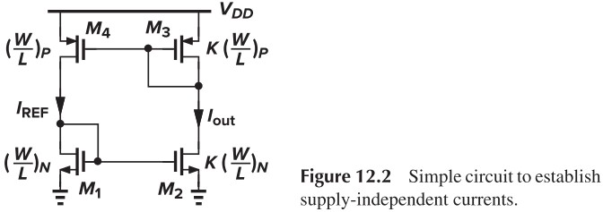
How do we calculate these currents? If $M_1$–$M_4$ operate in saturation and $λ ≈ 0$, than any current is possible! To uniquely define the currents, we add another constraint to the circuit (Fig. 12.3a)
%20Addition%20of%20RS%20to%20define%20the%20currents;%20(b)%20alternative%20implementation%20eliminating%20body%20effect.jpg)
由于 the sources of $M_1$ and $M_2$ are at different voltages, 所以 $V_\tx{TH1} = V_\tx{TH2}$ 实际上会存在误差。我们可以改用 Fig. 12.2b 的电路来消除这种误差。
由于上面均忽略了 channel-length modulation,所以我们一般用长沟道来制作这部分电路,同时这也会减小 flicker noise (真不错!🥰)
但是!但是!这个电路还有一个问题!在启动时,电流为 0,所有的管子都不会打开!因此我们需要加上 $M_5$,这样就在 VDD、M3、M5、M2、GND 之间形成一条通路,就有电流啦!
%20Addition%20of%20start-up%20device%20to%20the%20circuit%20of%20Fig.%2012.3(a),%20and%20(b)%20illustration%20of%20degenerate%20point.jpg)
Temperature-Independent References
If two quantities having opposite temperature coefficients (TCs), for example $V_1,V_2$, we can choose $\alpha_1,\alpha_2$ such that:
\[\alpha_1 \frac{\p V_1}{\p T}+ \alpha_2 \frac{\p V_2}{\p T}=0\]so we can obtaining a reference voltage:
\[V_\tx{REF} = \alpha_1 V_1 + \alpha_2 V_2\\ \Rightarrow \frac{\p V_\tx{REF}}{\p T} = \alpha_1 \frac{\p V_1}{\p T}+ \alpha_2 \frac{\p V_2}{\p T}=0\]Negative-TC Voltage
The forward voltage of a pn-junction diode (i.e. base-emitter voltage of bipolar transistors) exhibits a negative TC. 下面我们来求 $\p V_{BE}/ \p T$
The forward current of pn-junction is
\[\begin{aligned} I_C &= I_S [\exp(V_{BE} /V_T)-1]\\ &\approx I_S \exp(V_{BE} /V_T)\\ &= I_S \exp(qV_{BE}/kT) \end{aligned}\\ \Rightarrow V_{BE} = \frac{kT}{q}\ln (I/I_S)\quad\]- $V_T \equiv \frac{kT}{q}$
- The saturation current $I_S \propto \mu k T n_i^2$ (参考 半导体物理器件 2.5 与 4.9)
- The mobility of minority carriers $\mu\propto \mu_0 T^m, m\approx -3/2$
- The intrinsic carrier $n_i^2 \propto T^3 \exp(-E_g/kT)$
Thus,
\[I_S = b T^{4+m} \exp \frac{-E_g}{kT}\\ b \tx{ is a prop. factor}\]Assume that $I_C$ is held constant. Thus
\[\frac{\p V_{BE}}{\p T} = \frac{\p V_T}{\p T} \ln \frac{I_C}{I_S} - \frac{V_T}{I_S} \frac{\p I_S}{\p T}\]其中,第一项为
\[\begin{aligned} \frac{\p V_T}{\p T} \ln \frac{I_C}{I_S} &= \frac{k}{q} \ln \left(\exp \frac{qV_{BE}}{kT} \right)\\ &= \frac{V_{BE}}{T} \end{aligned}\]第二项为
\[\begin{aligned} \frac{V_T}{I_S} \frac{\p I_S}{\p T} &= (4+m) \frac{V_T}{T} + \frac{E_g}{kT^2} V_T\\ &= \frac{(4+m)V_T+E_g/q}{T} \end{aligned}\]总的为:
\[\frac{\p V_{BE}}{\p T} = \frac{V_{BE}-(4+m)V_T-E_g/q}{T}\]At $T=300\tx{K}$, $\p V_{BE}/ \p T \approx -1.5 \tx{mV/K}$
Positive-TC Voltage
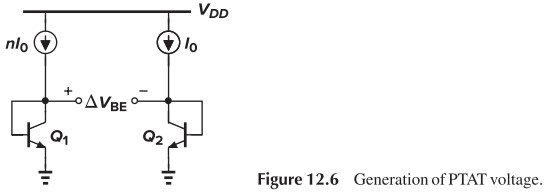
If two bipolar transistors operate at unequal current densities, then the difference between their base-emitter voltages is directly proportional to the absolute temperature.
感觉这样有点取巧,本质上就是负负得正嘛……
Example 12.2 要使 TC=+1.5mV/K 以抵消 BE voltage 的 TC($T=300K$),那么 $n$ 要取多大?
代入 $\dfrac{k}{q} \ln n = 1.5 \tx{mV/K}$,其中 $k/q = V_T/T = 0.087 \tx{mV/K}$,得到 $\ln n \approx 17.2$,即 $n = e^{17.2} = 2.95\times 10^7$
可见这个数很大,无法实现,所以需要修改电路。一种修改方法如下:

修改后,右边的 $I_0$ 减小为 $\dfrac{I_0}{m}$,从而加大左右电流相对的差异,变相“增大”了 $n$。相关公式修改为:
$$
\begin{aligned}
\Delta V_{BE} &= V_T \ln \frac{n I_0}{I_S} - V_T \ln \frac{I_0}{m I_S}\\
&= V_T \ln (nm)
\end{aligned}
$$
但其实这还不够,后面会讨论其他方法。
Bandgap Reference
With the negative- and positive-TC voltages obtained above, we can write $V_\tx{REF} = \alpha_1 V_{BE} + \alpha_2 (V_T \ln n)$. At room temperature, $\p V_{BE}/ \p T \approx -1.5 \tx{mV/K}$, and $\p V_{T}/ \p T \approx +0.087 \tx{mV/K}$, therefore
\[\alpha_1 \times (-1.5) = \alpha_2\ln n \times (+0.087)\]We choose $\alpha_1=1$ so that $\alpha_2\ln n = 17.2$, indicating that for zero TC
\[V_\tx{REF} \approx V_{BE}+17.2 V_T\\ \tx{一般基准电压为 1.25 V}\]Let us now devise a circuit that adds $V_{BE}$ to $\Delta V_{BE}$
Cosider the circuit shown in Fig. 12.8, $Q_2$ 是 $n$ 个管子并联,并且我们利用某种方法使得 $V_{O1}$ 和 $V_{O2}$ 相等。那么,我们有:
\[V_{O1} = V_{O2} = RI+V_{BE2}\\ \Rightarrow RI = V_{O1}-V_{BE2} = V_{O1}-V_{O2} = V_T \ln n\\ \Rightarrow V_{O2}=V_{BE2}+R_I = V_{BE2}+V_T \ln n\]我们可以利用运放来使 $V_{O1}$ 和 $V_{O2}$ 相等,即:
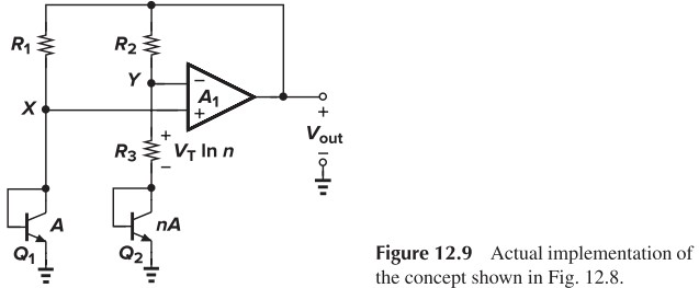
根据之前的分析,$\ln n(1+\frac{R_2}{R_3})$ 大约是 $17.2$,我们可以将 $\frac{R_2}{R_3}$ 取大一点,这样 $n$ 就不会太大。
但有时候运放会存在 Offset(失调电压),即下图中的 $V_{\tx{OS}}$,此时我们的参考电压会变为:
\[\begin{aligned} V_\tx{out} &= V_{BE2}+\frac{R_3+R_2}{R_3}(V_{BE1}-V_\tx{OS}-V_{BE2})\\ &=V_{BE2}+(1+\frac{R_2}{R_3})(V_T \ln n-V_\tx{OS}) \end{aligned}\]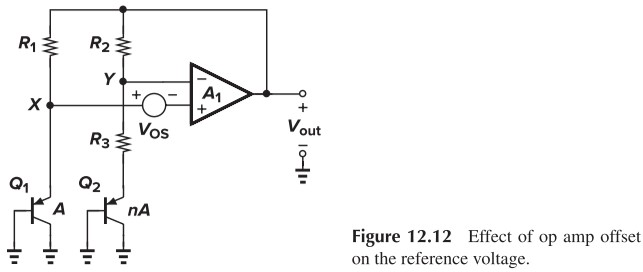
要减小 $V_\tx{OS}$ 的影响,就要增大 $V_T\ln n$,我们可以用下面的电路。注意到这个电路中有两点不同
- $R_2=mR_1$,这导致 $\Delta V_{BE}=V_T \ln(mn)$
- 下面串联了两个 BJT,这导致 $\Delta V_{BE}\times 2$
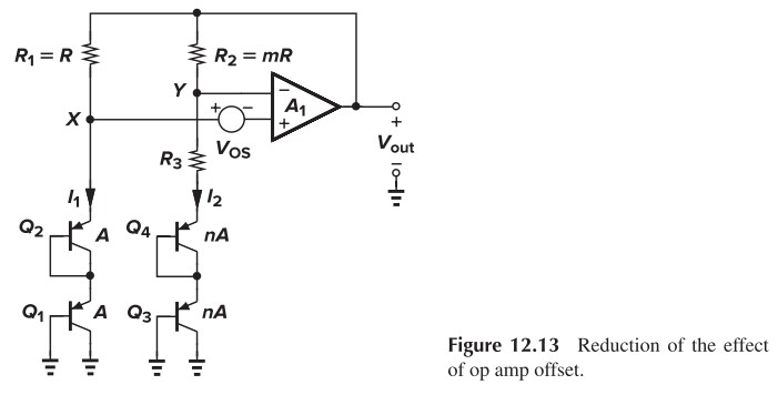
从而输出为:
\[\begin{aligned} V_\tx{out} &= V_{BE3}+V_{BE4}+\frac{R_3+R_2}{R_3}(2V_T\ln(mn))\\ &=2V_{BE}+(1+\frac{R_2}{R_3})[2V_T \ln (mn)-V_\tx{OS}] \end{aligned}\]