概论
运放有如下特点:
- high voltage gain
- high input impedance
- low output impedance
此外,还要考虑:
- speed
- output voltage swings
- power dissipation
我们一般用如下几个参数来描述运放。
- Gain
- Small-signal Bandwidth
- unity-gain $f_u$
- 3-dB frequency $f_{3-\tx{dB}}$
- Large-Signal Behavior
- Output Swing
- Linearity
- Noise and Offset: determine the minimum signal level that can be processed
- Supply Rejection
- Slew Rate: $V_\tx{out}$ 对时间的比值(输入阶跃,输出的最大斜率)
One-Stage Op Amps
Simple OTA
我们考虑下图中的 Simple OTA(operational transconductance amplifier)
根据前几章的知识,我们容易求出:
\[A_v = g_{m1} \frac{r_O}{2}\] \[\tx{if } {\rm r_{O2}=r_{O4}=r_O} \tx{ then}\\ \tx{BW}=\frac{1}{2 \pi \dfrac{r_O}{2}(C_L+C_{n1})}\]从而 $\tx{GBW}=\dfrac{g_{m1}}{2\pi(C_L+C_{n1})}$,$C_{n1}$ 指结点 1 处的电容。
这种结构的确定就是直流增益 $A_\tx{dc}$ 很难超过 40dB,所以我们采用下面的方法来增大输出电阻。
Telescopic Cascode Op Amps
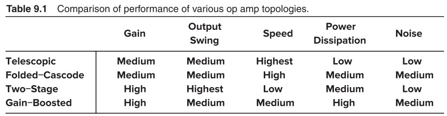
套筒式的优点就是输出阻抗放大了 $(g_m r_{DS})$ 倍,我们可以用下表来对比一下:
 |
|
| $$ \begin{aligned} A_v &= (g_m r_{DS})_1\\ R_\tx{out} &= r_{DS1} \end{aligned} $$ | $$ \begin{aligned} A_v &= (g_m r_{DS})_1(g_m r_{DS})_2\\ R_\tx{out} &= r_{DS1}(g_m r_{DS})_2 \end{aligned} $$ |
| $$ \tx{BW} = \frac{1}{2\pi R_\tx{out}C_L}\\ \tx{GBW} = \frac{g_{m1}}{2\pi C_L} $$ | |
 注意纵轴取了 log,$A_{v1}$ 和 $A_{v2}$ 实际是相乘而非相加。 |
|
可以看出,虽然增益增大,但仅增大低频增益,带宽反而减小了。
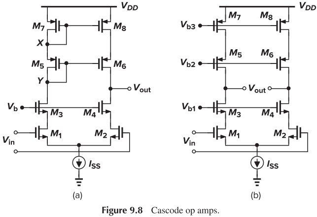
另外,the output swings of telescopic cascode op amps are limited. 我们考虑 Fig. 9.8b,output swing 为 $2[V_{DD}-(V_{OD1}+V_{OD3}+V_{ISS}+\vert V_{OD5} \vert + \vert V_{OD7} \vert)]$(总电压减去 overdrive 电压和电流源电压,2 是源于差分)这种缺陷在输入与输出短接时会更明显。我们考虑 Fig. 9.9
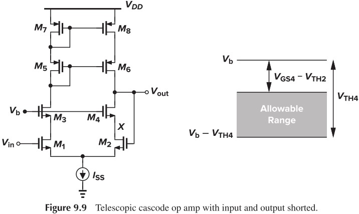
由于:
\[\begin{cases} V_\tx{out} \leq V_X + V_\tx{TH2}\\ V_\tx{out} \geq V_b-V_\tx{TH4}\\ V_X=V_b-V_{GS4} \end{cases}\\ \Rightarrow V_b-V_\tx{TH4} \leq V_\tx{out} \leq V_b-V_{GS4}+V_\tx{TH2}\\ \Rightarrow V_\max - V_\min = V_\tx{TH4}-(V_{GS4}-V_\tx{TH2})\]可见输出摆幅进一步被限制了。
Folded-Cascode Op Amps
the drawbacks of telescopic cascode op amps:
- limited output swings
- difficulty in choosing equal input and output CM levels
In order to alleviate the drawbacks, a “folded-cascode” op amp can be used.
%20Telescopic%20and%20(b)%20folded-cascode%20op%20amp%20topologies.jpg)
先对比大信号的特性。Two important differences between the two circuits in Fig. 9.14 are:
- (b) requires more bias current than (a)
- (a): $I_1,I_2$
- (b): $I_{SS},I_1,I_2$ which means that (b) consumes more power.
- (b) has a wider voltage swing, especially when input and output shorted.
- (a): the input CM level cannot exceed $V_{b1}-V_{GS3}+V_\tx{TH1}$
- (b): the input CM level cannot exceed $V_{b1}-V_{GS3}-\vert V_\tx{THP}\vert$
下面对比小信号增益。具体计算过程请看老师的 PPT,这里就不写了,反正都是用 $G_m R_\tx{out}$ 计算得出的。
\[折叠式:\\ \vert A_v \vert \approx g_{m1} \{[g_{m3}r_{O3}(r_{O1}\Vert r_{O5})] \Vert [g_{m7} r_{O7}r_{O9}]\}\\ 套筒式:\\ A_v \approx g_{m1}[(g_{m3}r_{O3}r_{O1})\Vert (g_{m5}r_{O5}r_{O7})]\]注意到式中,折叠式多了一个 $r_{O1}\Vert r_{O5}$,另外,PMOS 的 $g_{m1}$ 也比 NMOS 小,这导致它的增益比套筒式小 2~3 倍。
另外,折叠式输入端的电容也会比套筒式大,导致极点更趋近于低频(见下图)。
总结:the drawbacks of folded-cascode op amp:
- consumes more power 功耗大
- the gain is 2~3 times lower than telescopic cascode 增益小
- the pole is quite closer to the origin than that associated with the source of cascode devices in a telescopic topology 极点靠近原点,速度会变慢
为了增大电压摆幅,就不得不忍受这些缺点😕。
Two-Stage Op Amps
为了克服前面 one-stage op amps 的种种缺点,我们可以用 two-stage op amps. 第一个 stage 用来提供高增益,可以采用之前学过的各种高增益电路;第二个 stage 用来增大摆幅,一般采用简单的 CS stage。
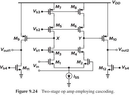
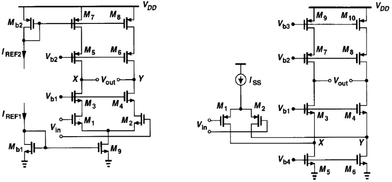
以 Fig. 9.24 的电路为例,它的增益如下:
\[A_v \approx {g_{m1,2}[(g_{m3,4}+g_{mb3,4})r_{O3,4}r_{O1,2}]\Vert (g_{m5,6}+g_{mb5,6})r_{O5,6}r_{O7,8}}\\ \times [g_{m9,10}(r_{O9,10}\Vert r_{O11,12})]\]输出电压摆幅为 $V_{DD}-\vert V_{OD9,10}\vert-V_{OD11,12}$
Gain Boosting
Basic Idea
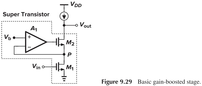
One-Stage Op 的增益不够,Two-Stage Op 的速度又太慢了(电容太大),为了解决这些问题,我们又提出了 Gain Boosting. 它的原理如下:在单个 CS Stage 前面再加一个放大器,并且将反相输入端和 S 是连在一起的
%20Transistor%20preceded%20by%20a%20voltage%20amplifier,%20and%20(b)%20equivalent%20circuit.jpg)
我们可以轻松算出增益为 $-A_1g_mr_O$,也就是说,原本的跨导只有 $g_{m}$,现在增大到了 $A_1g_m$
我们可以将这个结构看成是一个更牛逼的 MOS 管,并放到之前的电路中,比如下图中的 degenerated stage
%20transconductance,%20and%20(b)%20output%20resistance.jpg)
容易算出 $V_{GS} = (V_\tx{in}-R_SI_\tx{out})A_1 - R_S I_\tx{out}$ 且 $I_\tx{out}=g_m V_{GS}$,则:
\[G_m = \frac{I_\tx{out}}{V_\tx{in}}=\frac{A_1g_m}{1+(A_1+1)g_m R_S}\]注意到式子中,分子中的 $g_m$ 增大了 $A_1$ 倍,而分母中的 $g_m$ 增大了 $(1+A_1)\approx A_1$ 倍。
$R_\tx{out}$ 的计算如下:$I_{r_O}=\dfrac{V_X-R_SI_X}{r_O}$,且 $I_0 = (-A_1R_SI_X-R_SI_X)g_m$,从而:
\[I_X = (-A_1R_SI_X-R_SI_X)g_m + \frac{V_X-R_SI_X}{r_O}\\ \Downarrow\\ R_\tx{out} = r_O+(A_1+1)g_m r_O R_S+R_S\]由于 $G_m$ 和 $R_\tx{out}$ 均增大了,所以总的增益也增大了。
 考虑 Fig. 9.28 从源端看进去的电阻,计算过程与上面类似,在此直接给出结果: $$ R_X = \frac{R_D+r_O}{1+(A_1+1)g_m r_O} $$ 可以看出分母中的 $g_m$ 同样增大了 $(1+A_1)$ 倍。
再来看一个例子,这次将 Gain Boost 放到输出管上(Fig. 9.29),它的输出电阻和之前 degenerated stage 是类似的,而由于 M2 的源端电阻很小(参考上面例题),所以 $r_{O1}$ 几乎不分流,$I_{D1}=g_m V_\tx{in}$ 全部流到输出端,从而:
\[\begin{aligned} \vert A_v \vert &\approx g_{m1}\left[ r_O+(A_1+1)g_m r_O R_S+R_S \right]\\ &\approx g_{m1}g_{m2}r_{O1}r_{O2}(A_1+1) \end{aligned}\]看来 Gain Boost 用来放大输出电阻也挺好用的。
Circuit Implementation
虽然之前的 Gain Boost 都是用双端的 Op 来实现,但其实用单端的放大器就能实现。As shown in Fig. 9.32(a), if $I_1$ is ideal, then $\vert A_1 \vert=g_{m3}r_{O3}$, yielding $\vert A_v \vert \approx g_{m1}r_{O1}g_{m2}r_{O2}(g_{m3}r_{O3}+1)$
%20an%20NMOS%20CS%20stage,%20(b)%20a%20PMOS%20CS%20stage,%20and%20(c)%20a%20folded-cascode%20stage.jpg)
但 (a) 有一个坏处就是 P 点处的电压必须高于 $V_{GS3}$。为了增大摆幅,我们将 nmos 换成 pmos,即 Fig. 9.32(b),这样的话增益不变,但 $V_P=V_{GS1}-V_{TH1}$。
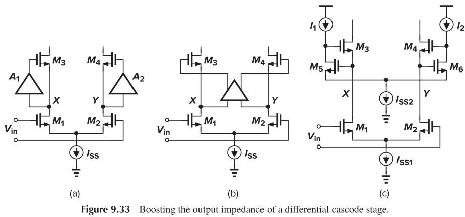
我们还可以进一步用在差分放大器上(Fig. 9.33),但具体分析我懒得写了。
Frequency Response
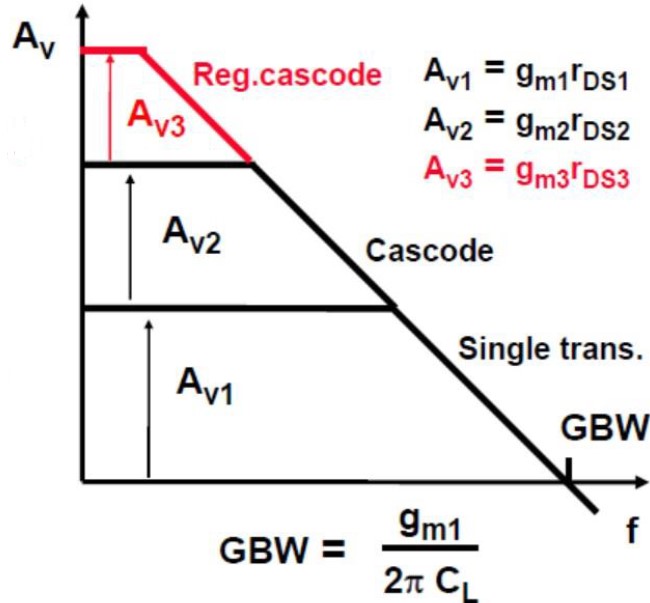
具体分析过程和之前分析频率响应是一样的,我这里就不写了,自己看书。从下图中可以看出 Gain Boosting 依然是增大增益、减小了带宽、GBW 不变。
小结
让我们回忆一下之前的内容:
我们嫌弃 CS Stage 的增益太小,于是用了 Cascode,多级 Cascode 就是 Telescopic,但是多级会消耗太多裕度,所以用了 Folded-Cascode,但 Folded-Cascode 只是消除了输入管的裕度损耗,堆叠的输出管还是会消耗很多裕度,所以我们又用了 Two-Stage 来减小输出管的裕度损耗,同时也进一步增大了增益。但 Two-Stage 的速度又不够快,所以又用了 Gain-Boosted 实现高增益且速度较快。
可以看出,有得必有失。当我们解决一个问题时,另一个问题就会冒出来,所以要权衡得失。
吐槽:上表中最菜的就是 Folded-Cascode,摆幅没提高多少,速度和功耗反而没 Telescopic 好。那我们为什么要学啊(╯‵□′)╯︵┻━┻
Common-Mode Feedback
Basic Concept
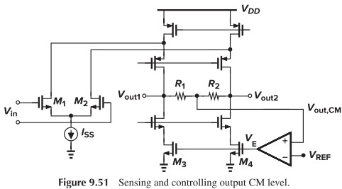
下面先来说说什么是 common-mode feedback (CMFB),为了让共模输出稳定,我们构造如下的共模反馈电路:
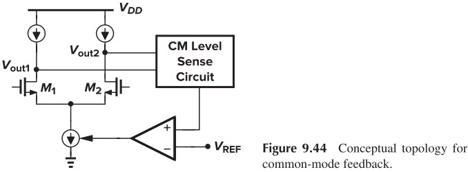
反馈电路包括三部分:
- sensing the output CM level
- comparison with a reference
- returning the error to the amplifier’s bias network
前两个还好理解,但第三个为什么反馈回 $I_{SS}$ 能使共模输出稳定呢?我们考虑下面这个 differential negative feedback
%20High-gain%20differential%20pair%20with%20inputs%20shorted%20to%20outputs,%20and%20(b)%20effect%20of%20current%20mismatches.jpg)
由于电流镜会存在误差,所以不可避免地,$I_{D3,4}\neq \frac{I_{SS}}{2}$,那么在 $X,Y$ 处,为了使上下电流相匹配,那么就会出现两种情况:
- $I_{D3,4}>\frac{I_{SS}}{2}$, M3 and M4 enter the triode region so that their drain currents fall to $I_{SS}/2$
- $I_{D3,4}<\frac{I_{SS}}{2}$, M5 enters the triode region, thereby producing only $2I_{D3,4}$
任意一种情况都是不我们希望的,所以我们需要调整 $I_{SS}$ 使其与 $I_{D3,4}$ 相匹配。
于是我们提出下图中的电路,其中,$R_1,R_2$ 负责获取共模电平,然后通过运放控制下面的偏置电流(当然,控制 $I_{SS}$ 也是可以的)。