Vacabulary
- crystalline
- X-ray diffraction
1.1 Silicon Srystal Structure
本节讲的是半导体晶体结构,首先要明白什么是“晶体”:
- A crystalline solid consists of atoms arranged in a repetitive structure, which can be determined by means of X-ray diffraction and electron microscopy.
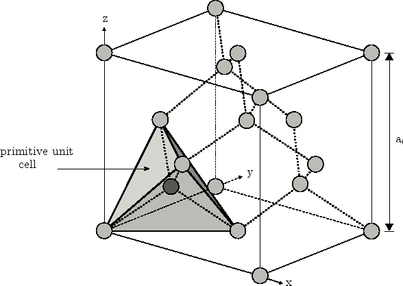
每种晶体我们都可以用 Basis + Lattice 来描述,Lattice 进一步可分为 unit cell,unit cell 进一步划分为 primitive cell,这两个词通常有很多种定义,书上的意思是 unit cell 是基本重复单元,而 primitive cell 是最小重复单元。有时候 primitive cell 不能反映对称性(比如硅的面心立方结构),所以常用 unit cell 来研究。unit cell 的边长称为 lattice constant,是个重要的参数。
硅的结构是 diamond structure,准确来讲是 FCC(Face Center Cubic),由于它有 4 个 valence electrons,与周围 4 个硅形成 4 个 covalent band,所以它的 primitive cell 的结构如下:
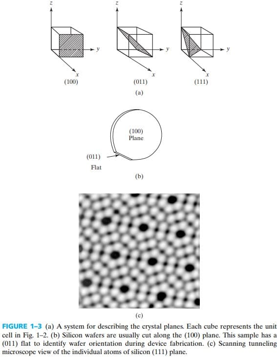
晶体有多个晶面,为了区分晶面的方向,我们取晶面在 x,y,z 轴上的截距的倒数作为晶向。比如 (abc) plane 就是与 x,y,z axes 交与 1/a, 1/b, 1/c lattice constants 的位置(注意单位是 lattice constants),括号里的 a b c 称为 Miller indices(密勒指数)。另外,用 [abc] 表示垂直于 (abc) plane 的方向,用于区分晶列的方向。
通常将 silicon wafer 沿着 (100) plane 切开成一片一片,这样能获得比较好的性能,同时沿着 (011) plane 切一个小口,用于标识方向。
1.2 Bond Model of Electrons and Holes
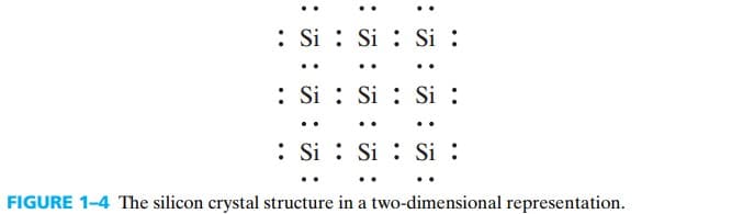
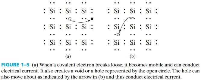
硅通过 4 个 covalent bond 与周围 4 个硅相连,如图 fig 1-4. 当然,这只适用于绝对零度时,此时没有 free electrons,不能导电;在其他温度下,thermal energy 会导致一部分 covalent electrons 挣脱而形成 conduction electrons,同时在原来的位置留下一个 hole,如图 fig 1-5. conduction electrons 和 holes 都能形成 conduct current.
通过测量产生 photoconductivity 时对应的 photon energy,可以推算出硅需要 1.1eV 才能产生一个 conduction electrons 和 holes. 而室温(27℃ or 300K)的 thermal energy $= kT = 0.26$ mV,所以室温下本征硅的 conduction electrons 和 holes 都比较少。
要增加载流子,可以通过 doping 引入 impurity atoms,根据杂质原子的族可以分为:
- donors:group Ⅴ elements, donate electrons and generate N-type semiconductors, e.g. As
- acceptors:group Ⅲ elements, accept electrons and generate P-type semiconductors, e.g. B
氢原子电离能 The ionization energy of a hydrogen atom is:
\[E_\text{ion} = \frac{m_0 q^4}{8 \varepsilon_0^2 h^2} = 13.6 eV\]As for silicon, we make some modification:
- replace the permittivity of free space $\varepsilon_0 $ with $\varepsilon_r \varepsilon_0=12 \varepsilon_0$ (12 is the relative permittivity of silicon)
- replace the free electron mass $m_0$ with a electron effective mass $m_n$
After the modification, 杂质在硅中的电离能 the ionization energy is about 50 meV, 大大小于热能,所以我们可以认为室温下杂质原子完全电离。
1.3 Energy Band Model
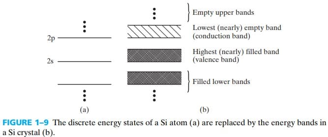
原子中的每个电子需要占据一个离散的能级,如果两个原子靠的很近,那么它们的每个能级就会分裂成两个。因为根据 Pauli exclusion principle(泡利不相容原则),每个能级只能容纳 2 个电子,而当原子靠得很近,它们的电子可能会共用,就可能出现一个能级上有 4 个电子的情况,为了避免这种情况,能级就会分裂。
在晶体中,有很多原子靠得很近,导致能级分裂成很多份,此时离散的能级 energy levels 就变成了连续的能带 energy bands,如图 fig 1-9
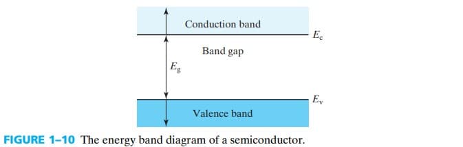
在晶体中,电子先填充 low energy bands,所以大部分低能带都是满的,再往上就会有一个几乎满的能带称为 valence band $E_v$,上面有个几乎空的能带称为 conduction band $E_c$,它俩之间的空隙称为 band gap $E_g$. 我们画能带图时,只画这三个部分,如图 fig 1-10。
band-gap energy 可以通过 measuring the absorption of light 来间接测量,当 $hv=E_g$ 时,光吸收比较强(具体可看 禁带宽度的测量 - 百度文库 (baidu.com) ),比如说:
EXAMPLE 1-1: Measuring the Band-Gap Energy
If a semiconductor is transparent to light with a wavelength longer than
0.87 µm, what is its band-gap energy?
SOLUTION:
$$
\begin{aligned}
h v &= h \frac{c}{\lambda} \\
&= 6.63 \times 10^{-34} {\rm (J\cdot s)}\cdot \frac{3\times 10^8
{\rm m/s}}{0.87 \unicode{x03BC} {\rm m }}\\
&=1.42 {\rm eV}
\end{aligned}
$$
Therefore, the band gap is 1.42 eV.
USEFUL RELATIONSHIP:
$$
hv ({\rm eV})=\frac{1.24}{\lambda (\unicode{x03BC} {\rm m })}
$$
常见半导体的禁带宽度如下:
| Semiconductor | InSb | Ge | Si | GaAs | GaP | ZnSe | Diamond |
|---|---|---|---|---|---|---|---|
| $E_g$(eV) | 0.18 | 0.67 | 1.12 | 1.42 | 2.25 | 2.7 | 6.0 |
1.3.1 Donors and Acceptiors in the Band Model
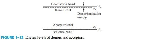
donors 的电离能比较小,也就是说 donor level $E_d$ 和 Conduction band 离得比较近;同理,acceptor level $E_a$ 和 Valence band 离得比较近。得到的能带图如下 fig 1-12
常见杂质的电离能如下:
| Donors | Acceptors | |||||
|---|---|---|---|---|---|---|
| Dopant | Sb | P | As | B | Al | In |
| Ionization energy(mV) | 39 | 44 | 54 | 45 | 57 | 160 |
上面杂质的电离能(在杂质中)相对而言比较小,被称为浅能级 shallow levels;某些杂质的电离能比较大(比如金),这类被称为深能级 deep levels。
1.4 Semiconductors, Insulators, and Conductors
The differences among semiconductors, insulators, and conductors are:
- Semiconductor has a nearly filled valence band and a nearly empty conduction band separated by a band gap.
- Insulator is similar to semiconductor except for a larger $E_g$
- Conductor has a partially filled conduction band.

补充一下,要导电的话导带就要半满,也就是能级上有奇数个电子(比如 Au, Al, Ag)。但有些偶数电子材料的也能导电(Zn, Pb),这是因为它们的 filled band 和 empty band 重叠形成了新的半满的能带,这类元素叫 semimetals
另外,半导体与绝缘体都是 has a filled valence band and an empty conduction band,区别只在于 $E_g$,但并没有一个明确的标准作为界限。
1.5 Electrons and Holes
对于 electrons 来说,能带越高对应的能量越大;而对于 holes,则是能带越低对应的能量越大。书上有个很好的比喻:「 We may think of holes as bubbles in liquid, floating up in the energy band. Similarly, one may think of electrons as water drops that tend to fall to the lowest energy states in the energy band.」
1.5.1 Effective Mass
当外加 $\mathscr{E}$ 的电场时,电子和空穴会获得一个加速度:
\[\begin{align} a&=\frac{-q \mathscr{E}}{m_n} \qquad \text{electrons}\\ a&=\frac{q \mathscr{E}}{m_p} \qquad \text{holes} \end{align}\]电子和空穴使用的是有效质量 effective mass ($m_n,m_p$)(考虑了一些微观效应)。典型值如下:
| Si | Ge | GaAs | InAs | AlAs | |
|---|---|---|---|---|---|
| $m_n/m_0$ | 0.26 | 0.12 | 0.068 | 0.023 | 2.0 |
| $m_p/m_0$ | 0.39 | 0.30 | 0.50 | 0.30 | 0.3 |
综合来看,空穴的有效质量比电子大一点,这是空穴和电子的迁移率不同的原因之一。
有效质量可以从波动方程中推出,但这有点复杂,我们直接给出结论:
\[\text{Effective mass } m^* \equiv \frac{\hbar^2}{\dif^2 E/ \dif \bd{k}^2}\]其中,$E$ 是电子能量,$\bd{k}$ 是波矢(用于描述波的振动),$E-\bd{k}$ 之间存在一定关系。我个人觉得这个公式有点像 $m = \frac{F}{\dif^2 v/ \dif t^2}$
不同半导体有不同的 $E-\bd{k}$ 关系,从而有不同的有效质量。
1.6 Density of States
前面说过能级分裂得到能带,能带说是连续的,但还是有疏密之分。单位体积的半导体中,某一个能量范围内的能级数目就叫 density of states:
\[D(E) \equiv \frac{\text{number of states in } \Delta E}{\Delta E \times \text{volume}} \;\mathrm{cm^{-3}\cdot eV^{-1}}\]这里直接给出 conduction-band density of states 和 valence-band density of states 的表达式(推导过程在书上的附录):
\[D_c(E) = \frac{8 \pi m_n \sqrt{2 m_n(E-E_c)}}{h^3}, \quad E \geq E_c\\ D_v(E) = \frac{8 \pi m_p \sqrt{2 m_p(E_v-E)}}{h^3}, \quad E \leq E_v\]
知道有多少能态,就能进一步求解有多少电子。
1.7 Thermal Equilibrium and the Fermi Function
在一定 thermal agitation 下,电子会电离,并跃迁到高能级。当然电子不可能无限跃迁,最终会形成 thermal equilibrium。
thermal equilibirium 并不是说电子就静止在导带上,它依然有一定概率再跃迁到其他能级,因此这是一种动态平衡。
在热平衡下,只能用概率来描述某个能级被电子占据的概率。我们认为这个概率满足 Fermi-Dirac distribution function:
\[f(E)=\dfrac{1}{1+e^{(E-E_F)/kT}}\\\]$E$ 是某一能级,$E_F$ 是 Fermi energy 或 Fermi level. 在一定温度下费米能级是固定的。在费米能级处,$f(E)=0.5$,如果费米能级越高,显然,电子占据高能级的概率就越大(也就是电离程度越大)
当 $E-E_F \gg kT$ 时(即能级远离费米能级),分母中的 $1$ 就可以忽略,从而退化成 Bolzmann approximation:
\[f(E) \approx - e^{-(E - E_F)/kT}\]
另外,当能级未被电子占据时,就是被空穴占据,所以能级被空穴占据的概率为:
\[1-f(E)\approx e^{-(E_F - E)/kT}\]1.8 Electron and Hole Concentrations
知道了能级密度 $D(E)$ 相当于知道了有多少个能级,然后还知道每个能级上有电子的概率 $f(E)$。那么,某个能量范围内的电子数就是:
\[n = \int_{E_1}^{E_2} f(E) D(E) \dif E\]如果要知道导带中的 Conduction Election 的数量,只需要替换积分上下限:
\[\begin{aligned} n &= \int_{E_c}^{\infty} f(E) D(E) \dif E\\ &= \frac{8 \pi m_n \sqrt{2 m_n}}{h^3} \int_{E_c}^{\infty} \sqrt{E-E_c} e^{-(E-E_F)/kT} \dif E\\ &= \frac{8 \pi m_n \sqrt{2 m_n} }{h^3} (kT)^{3/2} e^{-(E_c-E_F)/kT} \int_{0}^{\infty} \sqrt{E-E_c} e^{-(E-E_c)/kT} \dif (E-E_c) \end{aligned}\]由于 $\int_0^\infty \sqrt{x} e^{-x} \dif x = \sqrt{\pi}/2$,所以上式可以化简成:
\[n=N_c e^{-(E_c-E_F)/kT} \tag{1.8.5}\\ N_c \equiv 2 \left[\frac{2\pi m_n kT}{h^2}\right]^{3/2}\]$N_c$ is called the effective density of states(有效态密度)。 It is as if all the energy states in the conduction band were effectively squeezed into a single energy level, $E_c$, which can hold $N_c$ electrons (per cubic centimeter).
空穴也有类似的公式:
\[p = N_v e^{-(E_F-E_v)/kT} \tag{1.8.8}\\ N_v \equiv 2 \left[\frac{2\pi m_p kT}{h^2}\right]^{3/2}\]常用的 $N_c,N_v$ 取值如下:
| $T=300K$ | Ge | Si | GaAs |
|---|---|---|---|
| $N_c {\rm (cm^{-3})}$ | $1.04\times10^{19}$ | $2.8\times10^{19}$ | $4.7\times 10^{17}$ |
| $N_v {\rm (cm^{-3})}$ | $6.0\times 10^{18}$ | $1.04\times 10^{19}$ | $7.0\times 10^{18}$ |
注意:上面的公式只适用于 $E_F$ 离 $E_c,E_v$ 较远的情况,也就是 $n,p$ 较小的情况。一旦 $>10^{19} \text{cm}^{-3}$,就要用 Fermi-Dirac 分布计算。
By the way, 这节中的 $m_n,m_p$ 是 density-of-states effective mass,而 1.5 节中的是 conductivity effective mass,这俩个有效质量在数值上略有不同,但貌似考试中当成是一个东西。
1.8.1 Fermi Level and the Carrier Concentrations
注意到费米能级离 $E_c$ 或 $E_v$ 越近,导带 或 价带上的电子/空穴就越多。那么反过来,参杂浓度越大,费米能级离 $E_c$ 或 $E_v$ 越近。

EXAMPLE 1–3 Finding the Fermi Level in Si(计算费米能级)
Where is $E_F$ located in the energy band of silicon, at 300K with $n = 10^{17} \text{cm}^{–3}$?
And for $p = 10^{14} \text{cm}^{–3}$?
对公式:$n=N_c \exp[-(E_c-E_F)/kT]$ 进行变形:
$$
\begin{aligned}
E_c-E_F &= kT \cdot \ln(N_c/n)\\
&=0.026 \ln(2.8 \times 10^{19}/10^{17})\\
&=0.146 \text{ eV}
\end{aligned}
$$
Therefore, $E_F$ is located at 146 meV below $E_c$.
同理,对于空穴,有:
$$
\begin{aligned}
E_F - E_v &= kT \cdot \ln(N_v/p)\\
&=0.026 \ln(1.04\times10^{19}/10^{14})\\
&=0.31 \text{ eV}
\end{aligned}
$$
Therefore $E_F$ is located at 0.31 eV above $E_v$.
注意:上面的公式只适用于 $E_F$ 离 $E_c,E_v$ 较远的情况,也就是 $n,p$ 较小的情况。一旦 $>10^{19} \text{cm}^{-3}$,就要用 Fermi-Dirac 分布计算。(重要的事要强调几次才行!!!)
1.8.2 The np Product and the Intrinsic Carrier Concentration
由于 $E_F$ 不可能同时靠近 $E_c,E_v$,所以 $n,p$ 不可能同时大。我们将 $n,p$ 相乘,得到:
\[np=N_c N_v e^{-(E_c-E_v)/kT}=N_c N_v e^{-E_g/kT}\]我们定义这个乘积为:
\[np=n_i^2 \tag{1.8.11}\\ n_i=\sqrt{N_c N_v} e^{-E_g/2kT}\]$n_i$ 称为 intrinsic carrier concentration,”intrinsic” 的中文是「本征的」,指的是无掺杂的情况。从这点可以看出,无论掺杂浓度多少,$np=n_i^2$ 只与温度有关。这个式子有点像高中的离子平衡。
对于本征半导体,$n=p=n_i$,此时的 Fermi Level 就叫 intrinsic Fermi level,本征费米能级的计算和上面的例题是一样的。
在半导体中,电子与空穴哪个多,就把哪个叫 majority carriers 多子,另一个就叫 minority carriers 少子。我们计算时只需要计算出多子,然后根据 $n_i$ 再将另一个算出来。
常见材料在 300K 下的本征载流子浓度如下:
| 300K | Si | GaAs | Ge |
|---|---|---|---|
| $n_i$ | $1.5\times 10^{10} \text{cm}^{-3}$ | $1.8\times 10^{6} \text{cm}^{-3}$ | $2.4\times 10^{13} \text{cm}^{-3}$ |
1.9 General Theogy of n and p
shallow donor and acceptor levels 同样满足 Fermi-Dirac 分布,所以上面的式子同样适用于施主、受主能级。
一般来说,shallow donor and acceptor levels 离 Fermi level 比较远,因此我们可以近似认为杂质全部电离,即:
\[n=N_d \text{ or } p=N_a\]上式仅针对单一杂质。如果同时存在施主和受主,那么根据电荷守恒,有:
\[\begin{aligned} &\begin{cases} n+N_a = p+N_d\\ np=n_i \end{cases}\\ \Rightarrow &\begin{cases} n=\frac{N_d-N_a}{2}+\left[ \left( \frac{N_d-N_a}{2} \right)^2+n_i^2 \right]^{1/2}\\ p=\frac{N_a-N_d}{2}+\left[ \left( \frac{N_a-N_d}{2} \right)^2+n_i^2 \right]^{1/2} \end{cases} \end{aligned} \tag{1.9.2}\label{1.9.2}\]- 若 $N_d - N_a \gg n_i$,即 N型,则可以忽略 $n_i$ 项,得到: \(\begin{aligned} n&=N_d-N_a\\ p&=n_i^2/n \end{aligned} \tag{1.9.3}\)
- 若 $N_a - N_d \gg n_i$,即 N型,则可以忽略 $n_i$ 项,得到:
\(\begin{aligned} p&=N_a-N_d\\ n&=n_i^2/p \end{aligned} \tag{1.9.5}\) 我们将上面两种杂质相互抵消的现象称为:dopant compensation 杂质补偿.
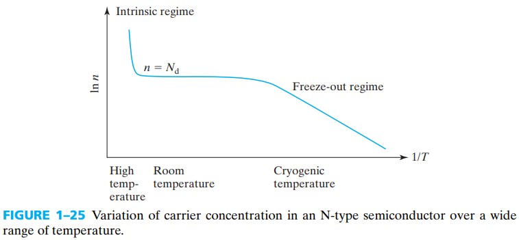
1.10 Carrier Concentrations at Extremely High and Low Temperatures
除了 1.9 中提到的杂质补偿,还有一种特殊情况就是当温度很高时,$n_i$ 很大,使得 $\eqref{1.9.2}$ 中仅留下 $n_i$ 项,从而:
\[n=p=n_i\]也就是说,在高温下,杂质半导体会变为本征半导体。
另一个极端就是当温度很低,不完全电离,这时 $E_F$ 会跑到 $E_d$ 之上(对于N型来说),此时的电子浓度为(analysis is complicated~):
\[n=\left[\frac{N_cN_d}{2}\right]^{1/2} e^{-(E_c-E_d)/2kT}\]这种现象称为 freeze-out,器件在这种情况下工作时,能达到 low noise and high speed 的效果,所以我们经常看到网上有人用“液氮”来超频。
总的来说,$n$ 与 $T$ 的关系如下: